Summary
We decided to investigate the potential of soft-switching the input buck stage of the Littlebox inverter in order to increase efficiency and reduce the overall footprint. Our investigation focused on the quasi-square wave (QSW) topology. We began by sizing and selecting the components, followed by simulation in SPICE and controller design in MATLAB using the selected components. In SPICE, we controlled the timing of the switching of the high- and low-side FETs through non-linear dependent elements (“B elements”) and computed the switching losses to compare with the hard-switched baseline. In MATLAB, we implemented a PI control loop to generate a 240 Vrms, 120 Hz rectified sine wave as our desired buck stage output waveform. With our chosen components, we were able to decrease the footprint of the buck stage from 642.25 mm2 to 496.31 mm2. The power loss for a 240 V DC output, however, increased from 37.5 W to 55.0 W.

Figure 1: Circled is the buck stage of the current iteration of the Littlebox inverter.
What We Did
Component Sizing and Selection
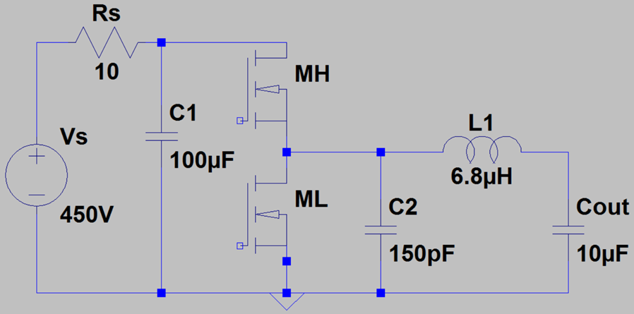
- For the selection of our high FET (MH), the key criterion is that VDS,max has to be greater than 450 V because when MH is off and low FET is on, the voltage difference across MH will be 450. Another criterion we had is that the FET should be able to withstand more than 18 A as this is expected high current threshold at the peak of the rectified sine wave (240V), which is the worst case scenario or max current. Given these criteria, we looked
at Infineon ThinPak 8x8 series as it is known to have small footprint. We chose the FET, IPL60R199CP , which has the following specifications.
- VDS,max = 600 V, ID,max = 16.4 A, RDS,on = 0.199 Ω
- td,on = 10 ns, td,off = 50 ns, trise/fall = 5 ns
- Similarly, as the low FET (ML) has to be able to withstand the maximum voltage difference of 450V (when Vx is charged to 450V and ML is grounded) we chose the same Infineon FET, IPL60R199CP, to be our low FET. The footprint of this FET is 8x8 mm2.
- For our inductor, our key criterion is that saturation current Isat has to be greater than 18 A so we used
Coilcraft’s Power Inductor Finder to find an inductor between 5uH and 20 uH with minimum footprint while meeting our current saturation criteria. Our chosen inductor is DO5040H-682, which has the following specifications.
- L = 6.8uH, Isat = 22.5 A, Footprint = 363.19 mm^2
- We used the equation, 1⁄2*LI^2=1⁄2*CV^2 where V is 450V (voltage the cap needs to charge up to so that MH can be turned on ZVS) and I is the minimum reverse current, which we set at -2. The expected capacitor size is approximately 134 pF but since there is no capacitor that is exactly that size, we chose a ceramic capacitor from Digikey (445-2337-1-ND) which is 150 pF. We expect the reverse minimum current to be around -2.11 A. It also has a rated voltage of 630, which is more than sufficient for the maximum expected voltage drop of 450 V.
Controller Design in MATLAB
- Since the voltage across the output capacitor is dependent on the average inductor current, we used the high current threshold as our key control variable.
- We stored the values of one period of the desired rectified sine output waveform in an array, and used this as our reference voltage input to our controller.
- Our controller is a PI control loop that is called at the start of every switching cycle and sets the high current threshold for that cycle based on the reference voltage input for that time step as well as its deviation from the current sampled output voltage.
- In addition, we included the effect of source resistance in our simulation.
What We Learned
Component Selection
For the high-side FET, one issue we found is that the maximum continuous drain current of the chosen FET is 16.4 A, which is less than the 18 A peak inductor current we obtain when producing a 240 V DC output in our SPICE simulation. However, the current through high-side FET only exceeds 18 A for such a short amount of time within a cycle, and the peak inductor current only exceeds 16.4 A during cycles when output voltage is close to maximum, so that this was effectively similar to a pulsed current. With our chosen FET able to take a maximum pulsed drain current of 51 A, we expect it to be able to handle this excess inductor current.
MATLAB
When we tried to model the source resistance, we found that the controller was quite sensitive to the resistance values and was unable to run properly for values above 6 ohms as one or more of the soft-switching requirements (e.g. v_x reaching v_s - i_l*r_s) were not met. The natural resonant frequency of our tank circuit (4.98 MHz) is also much higher than the switching frequency (average 748 kHz), and it was difficult to verify that the resonant stages of the quasi-square wave were actually sinusoidal segments.
SPICE
For both SPICE simulations, we used B elements as the gate drives to our buck converter’s switches. Using the unit step function, we constructed rules for when each switch should turn on and off. Our conditions properly determine when each switch should turned on or off to achieve soft-switching (ZVS), but we had trouble writing appropriate boolean expression to differentiate between sections of a switching cycle. After trying to solve the problem with another B element acting as memory, we finally realized it would be impossible to switch at zero voltage without some millivolt deviations. After calculating what those deviations would be, the next problem was getting the B element to turn up its voltage fast enough to turn on/off the switches fast enough. The solution was to alter the B elements tripdv and tripdt parameters which act to varying the element’s sensitivity to changes in the simulation. Once properly adjusted, the B elements served as effective gate drives for the switches. Another issue of note is that after running the simulation for several hundred of microseconds, the poor open loop control of the simulation causes converter to eventually end up oscillating in the resonant stage. This can be remedied by implementing closed loop control in the future.
Key Results
Footprint of Components
The following table is a summary the footprint comparison of the buck stage of the Littlebox inverter with and without the QSW topology.
| Footprint (square mm) | Hard-switched | Soft-switched |
|---|---|---|
| Cx | N.A. | 5.12 |
| Inductor | 342.25 | 363.19 |
| High-side switch | 150 | 64 |
| Low-side switch | 150 | 64 |
| Overall buck components footprint | 642.25 | 496.31 |
MATLAB Results
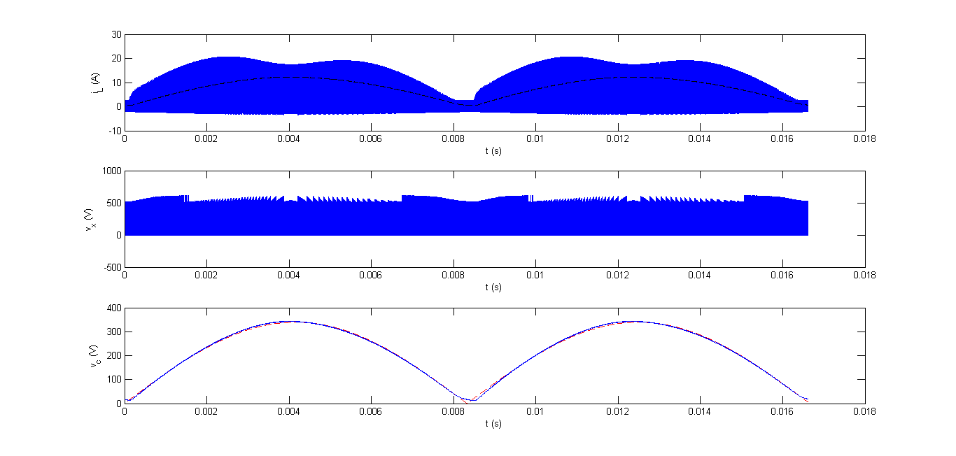
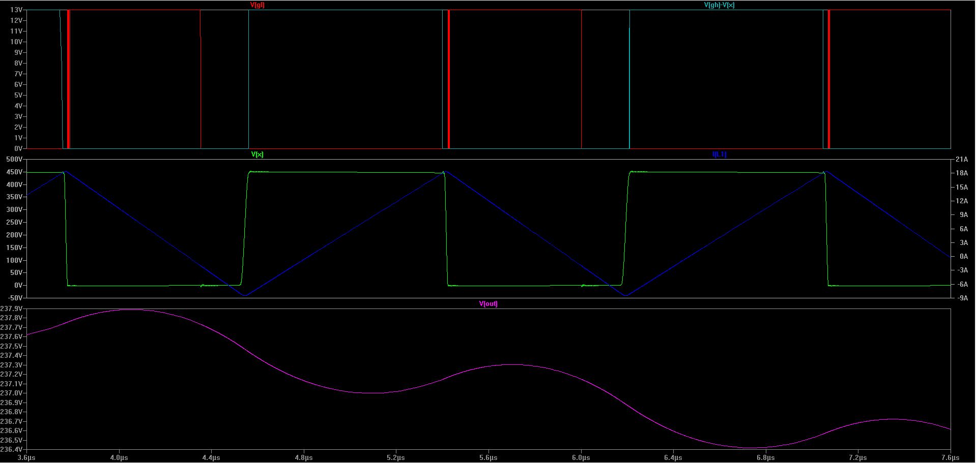
Our output voltage waveform shows good tracking of the desired 240 Vrms, 120 Hz rectified sine wave, with small deviations at low output voltage. This is likely due to the output capacitor not being able to charge and discharge quickly enough to track the sine wave at its steepest point. The inductor current has a ripple from -3.4 A to 20.7 A, with an average of 7.8 A.
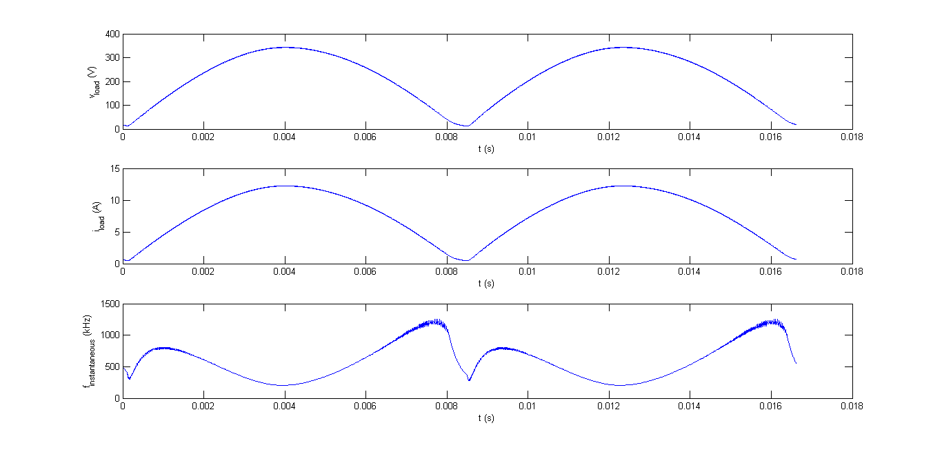
The instantaneous frequency varies from 70 kHz to 1.25 MHz with an average of 748 kHz. The load current goes from 0 A to 12.3 A with an average of 7.7 A.
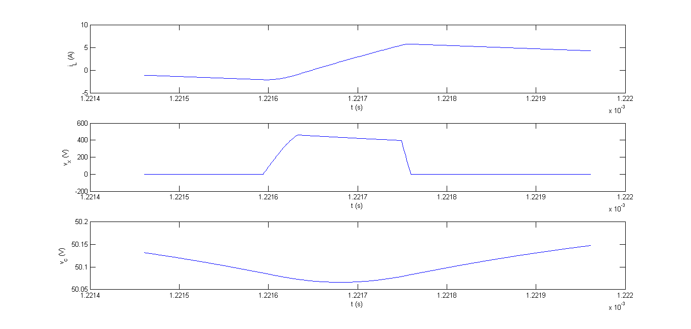
The above closeup of the output voltage waveform while it in ramping up along rising part of the rectified sine wave show the two resonant segments of the quasi-square wave. The effect of source resistance can be seen as inductor current ramps up between the resonant segments.
SPICE waveforms
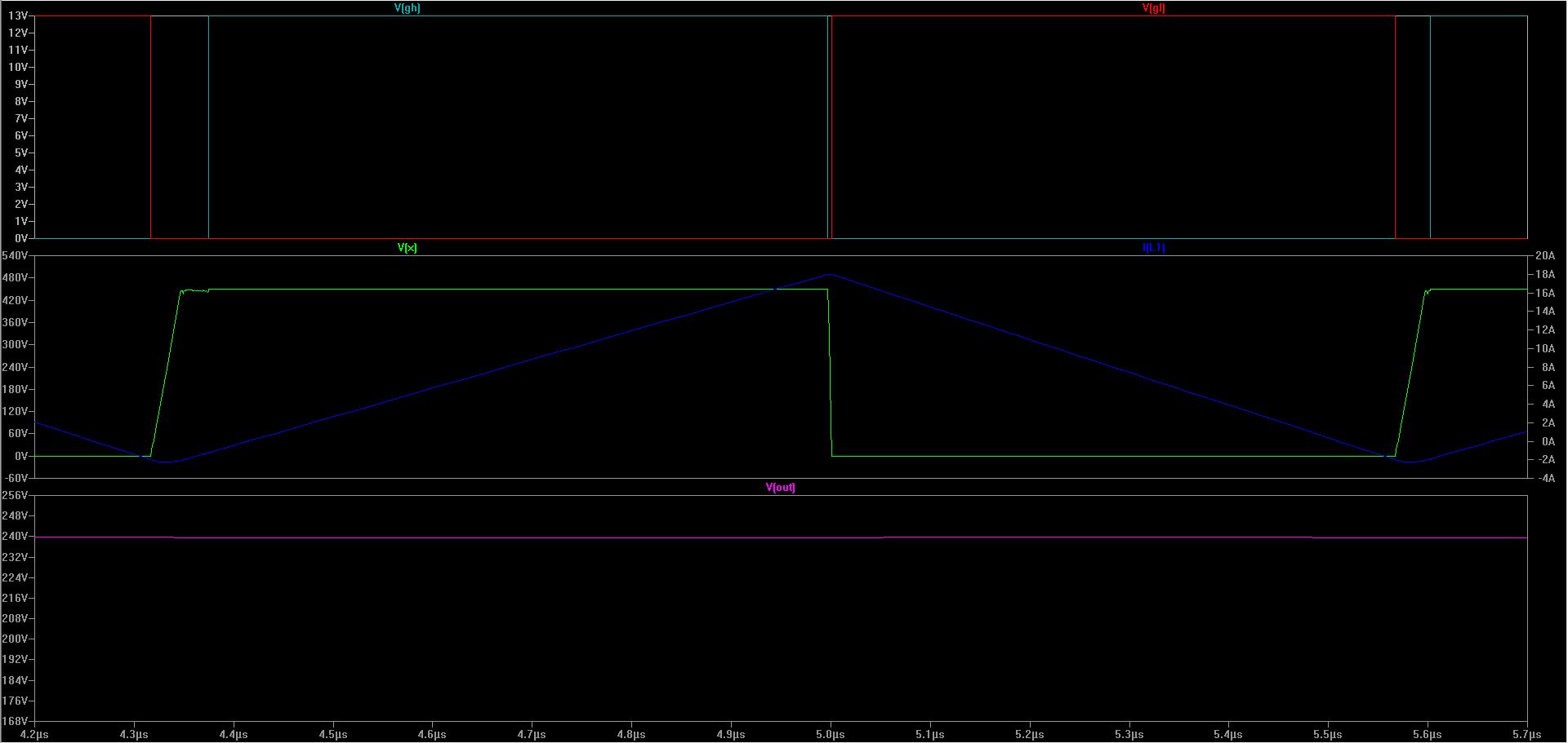
Ideal switches used here. B elements on the gates look for transition events to turn the switches on and off.
Simulation with provided Spice model of Infineon FET. Note the FET’s turn off time between when the low FET gate turns off and when current rises to charge the capacitor
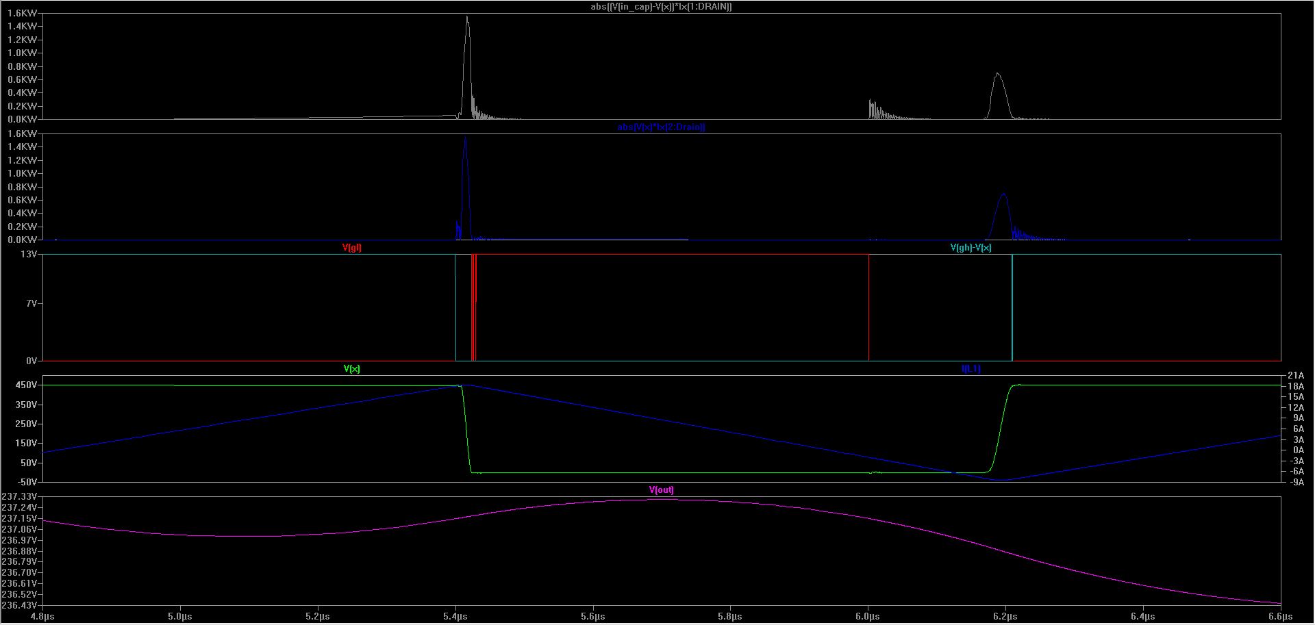
Showing the simulated switching losses through the MOSFETs. Note the peculiar hump of power loss thru the top side FET that occurs when the low side FET turns on.
Power Loss
Based on our simulations using Infineon’s SPICE model of the IPL60R199CP power MOSFET, in one switching cycle of outputting the peak 240 V, we obtain 50.57 μJ of energy loss through the top FET and 39.80 μJ through the bottom FET. With a cycle time of 1.66 μs, thus a frequency of 602.4 kHz, our total switching losses are 54.44 W. Since the peak power loss of M1 and D1 of Littlebox when it is hard-switched is 37.50W, our losses with soft-switching are greater than the hard switching power loss calculation above and does not make sense. We believe that some of this additional loss stems from a power hump through the top side switch that occurs when the low side switch is turn off. However, that hump is only 15.65 μJ and thus discounting its effect only improves switching losses down to 45.06 W. Regardless, more investigation needs to be performed to pinpoint the current issue, no pun intended.
Description of Deliverable
Please refer to the Key Results section for a detailed explanation of our results and Appendix A for the netlist that we used to get our SPICE simulations.
Next Steps
Through both our MATLAB and SPICE simulations, we have sufficient evidence to believe that soft-switching the buck stage can benefit the Littlebox by minimizing both footprint and losses. Given that we did not investigate different suppliers for the components, it would be worthwhile to investigate components from other vendors as they may potentially have smaller footprints. This search could be particularly worthwhile for further minimizing the size of the inductor. Furthermore, in terms of our SPICE model, we were only able to simulate with models the Infineon FET. It would also be interesting to add real inductors and capacitors into the simulation. For the controller design in MATLAB, we could investigate making the low current threshold a variable dependent on the output voltage in order to reduce the current ripple.
Appendix
References and Resources
Soft-Switching, EE 152 Notes, Bill Dally; Coilcraft; Infenion; Vishay