GaN FET Buck Converter
EE 155/255 Fall 2015
Spencer Gibbs, Jacob Baldwin, Jonathan Wilkins
Project Overview
In power electronics, one of the main goals is to maximize converter efficiency while meeting performance specifications. The purpose is not so much to avoid wasting energy, but because for high power applications, small percentages of loss mean large amounts of heat that must be dissapated by bulky, expensive cooling systems. Perhaps the largest source of loss in switching converters is in the switching and conduction losses found in the switching transistors. In this project we experiment with a new type of power transistor, the GaN FET, for improving effiency in a simple buck converter. The GaN FET is an ideal transistor for low to medium power applications because it has a very small gate charge and no reverse recovery charge, leading to rapid switching times and reduced switching losses.
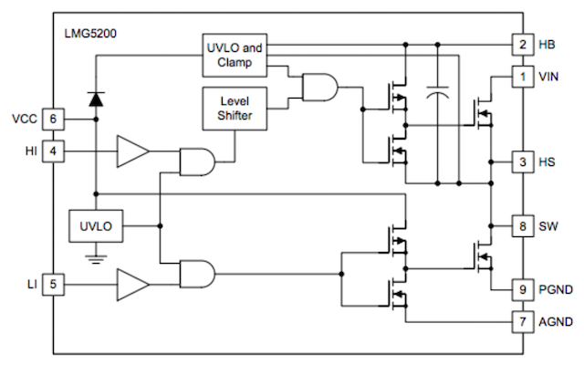
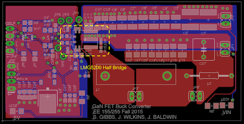
LMG5200 80V Half Bridge
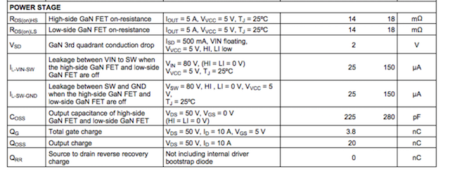
The reason GaN FETs help reduce losses in switching converters is one of several reasons they are tricky to use: high current transients. Suppose we are switching 100V, and driving 1A into the gate of a GaN FET that has a gate charge of 3.8 nC. It will take 3.8 nS to charge the gate, during which the impedance ramps linearly from 0 to Ron = 18mOhms, or 14.62 S/ns. Then the current ramps at dI/dt = (100V)(14.62) = 1462 A/ns. With this dI/dT, every nH of parasitic inductance generates a whopping 1.462kV! The same inductance causes the current to ramp at something much less, but the point is clear: every nH of parastic inductance in the switching loop counts.
A second consideration when driving GaN FETS is their suseptablilty to failure due to transients on their gates. Even a short pulse above 7V can damage the FET, so protection circuits must be built in to ensure save voltages at their gates.
With this in mind, we decided to use the LMG5200 80V integrated GaN FET half bridge module from Texas Instruments, shown above. Because the module places both high and low transistors on the same die, parasitic inductance along the switching node is minimized. Additionally the module incorporates a GaN FET gate driver and protection circuitry, which, given the limited time frame for this project, seemed important to improve our odds of success.
Below are the power stage specs for the LMG5200. Note the 3.8 nC gate charge and 0 nC reverse recovery charge... these are the main reasons to use GaNs.
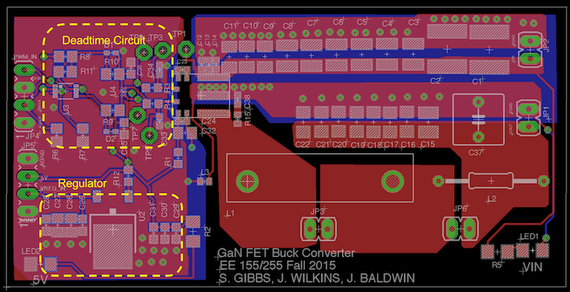
Deadtime Circuit

To prevent shoot through conditions we need to ensure the high transistor is never on when the bottom is also on. The deadtime circuit above provides this offset. First PWM signal passes through a buffer A1 to prevent loading on the driving microcontroller. An inverting buffer is used out of convenience because of the need for another inverter A2 which splits the signal into high and low levels. Then the signal passes through the RC filter on either side. The diode allows the signal on each side to rise much faster than it falls. Finally the signal is buffered again by inverters A3 and A4 and sent to the half bridge.
The RC time constant on each side sets the delay between the high side turning off and the low side turning on, and vice versa. Initially using R = 47 and C = 100p the time constant was set to 4.7 nS.
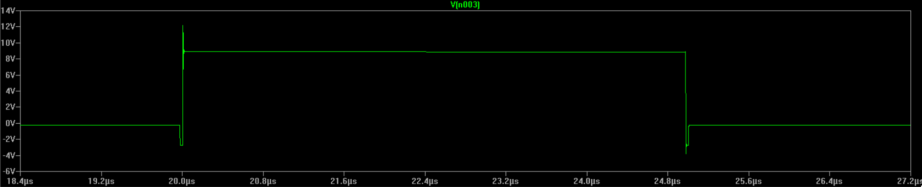
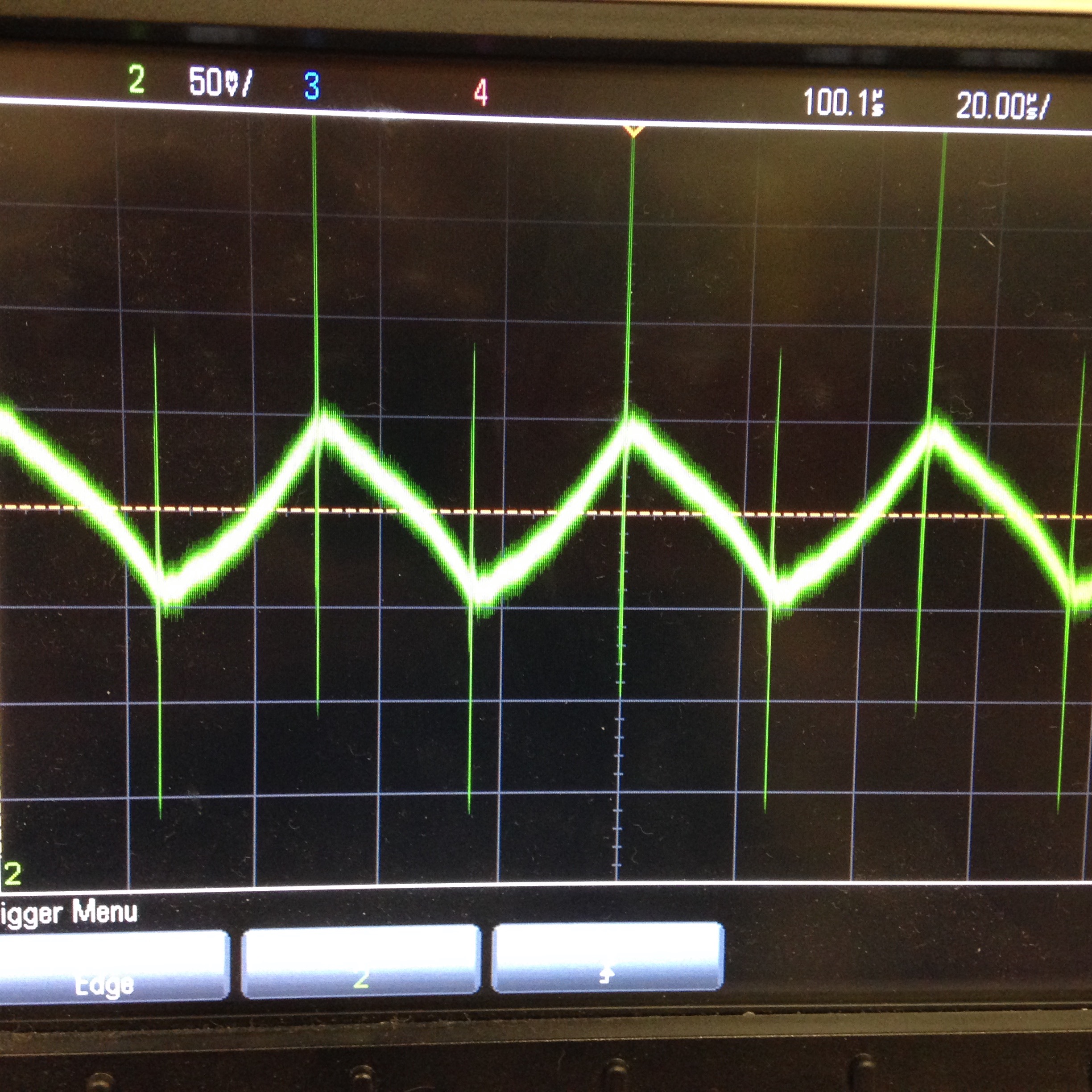
Simulation
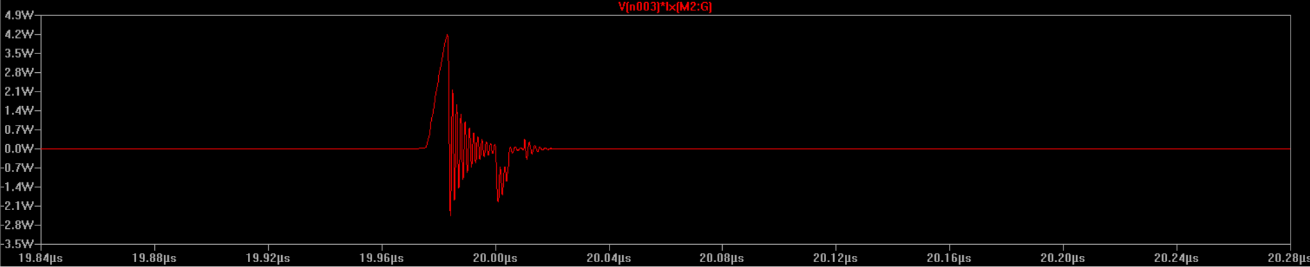
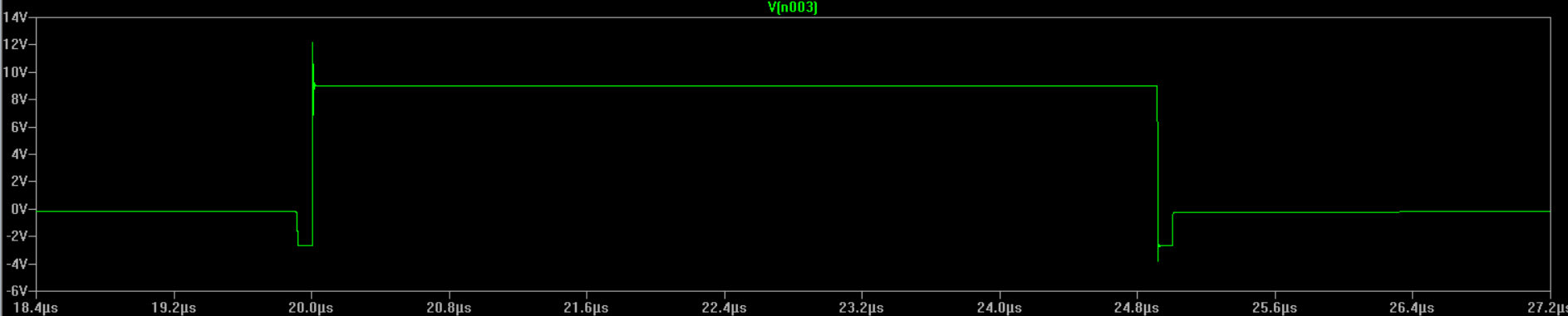
To get an idea how the circuit should perform, we simulated the circuit in Spice. We measured the efficiency of the simulation at different frequencies, but using a low dead time, because this should be most efficient. At 100 kHz, the input power was 2.41 W and the output power was 2.34 W, making the efficiency 97.1%. At 200 kHz, the input power was 2.43 W and the output power was 2.35 W, making the efficiency 96.7%. The pictures below show some traces from simulation.
Schematic
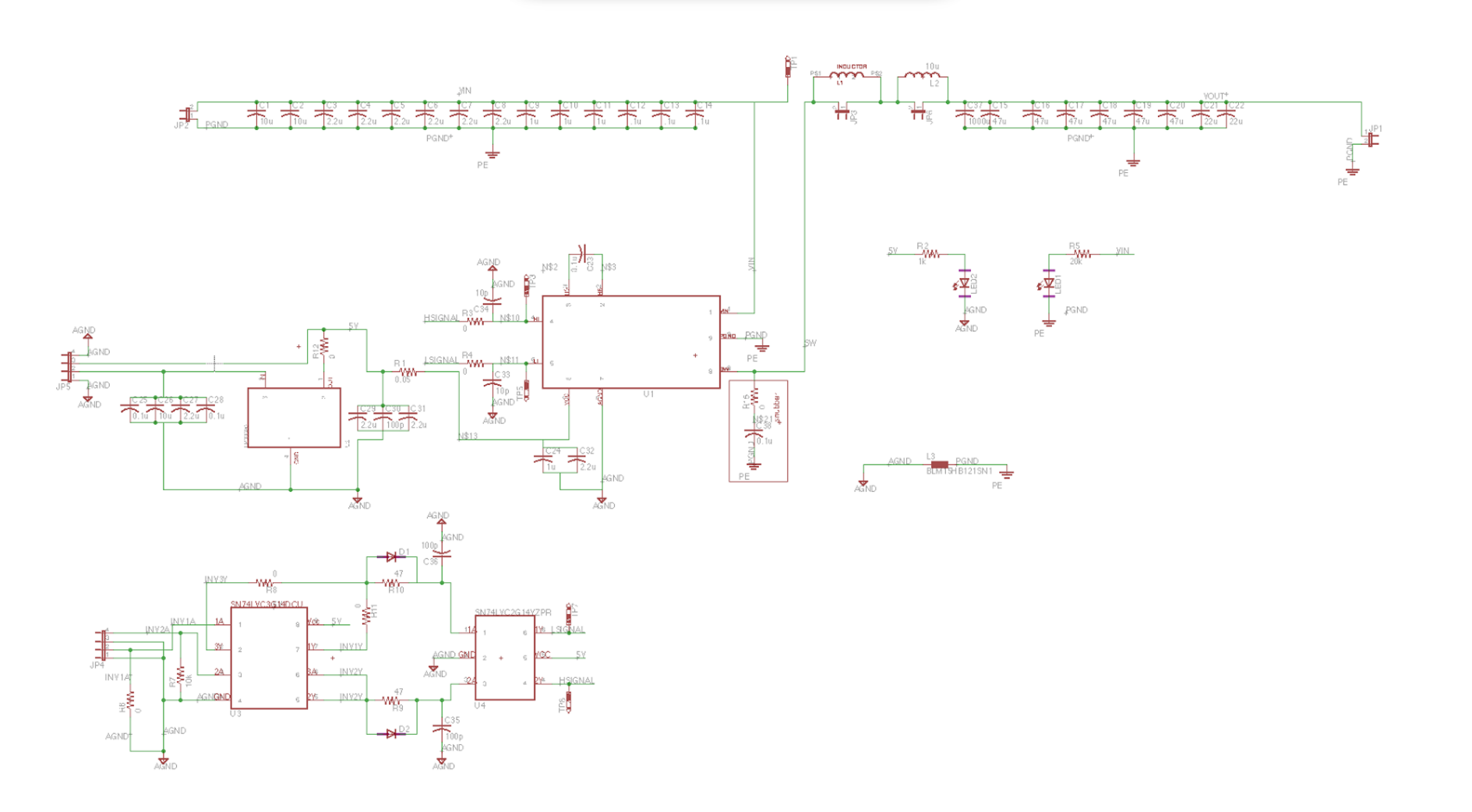
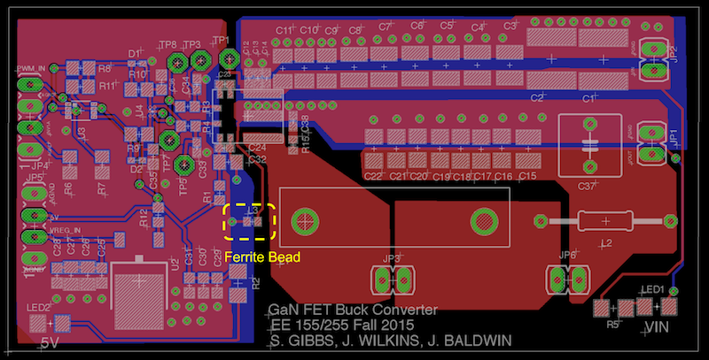
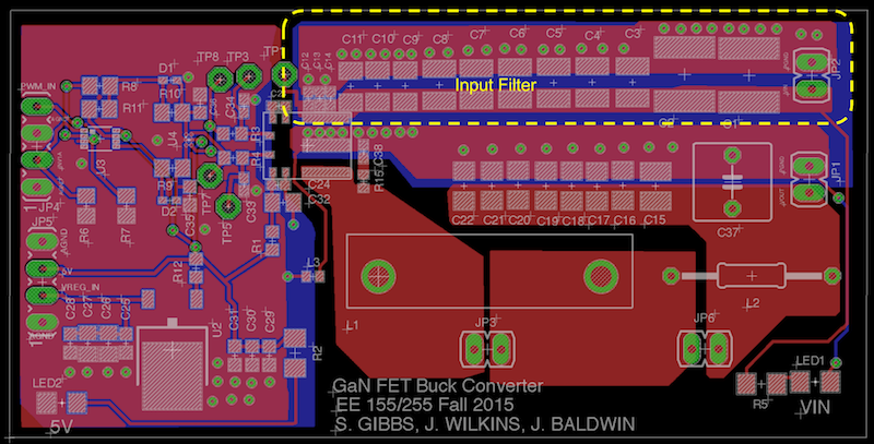
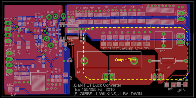
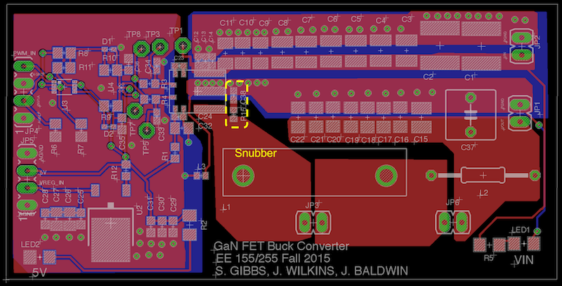
Our final schematic(2) is shown above. It is based on the suggested design by Texas Instruments. It includes a 5V regulator, a large array of input ceramic filter capacitors, output filter, separate power and analog grounds, a snubber for removing excess energy from the switching node in case of inductive parasitics, and the deadtime control circuit. To isolate switching noise from the digital control side, the power and analog grounds are separated by a ferrite bead.
PCB Layout Considerations
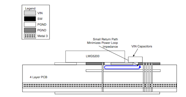
Switching Current Loop (4 Layer Board) (1)
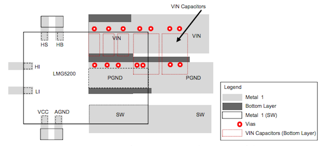
Recommended Layout (2 Component Layers) (1)
Perhaps the most important aspect of this project was a careful layout of the PCB. As shown above, the LMG5200 pads are laid out such that the input power rail and power ground are located right next to each other. The parasitc inductances we are conserned about lie in the loop between the supply capacitors, and the drain of the high transistor and source of the low transistor. By placing the smallest (high frequency filtering) capacitors immediately next to the VIN pad, the current loop is limited to the small region shown by the blue arrow. Placing the power ground return plane in layer 2 also reduces return path length. Additionally, the anti-parallel flow of the current reduces EMI emission by creating a net zero current along that axis.
A second parasitic to consider is the capacitance on the switching node SW. In order to reduce this capacitance we eliminate any metal in the layers below the pad between the SW node and the output inductor. Additionally we try to place the output inductor close to the switching node to reduce resistance and capacitance on that node.
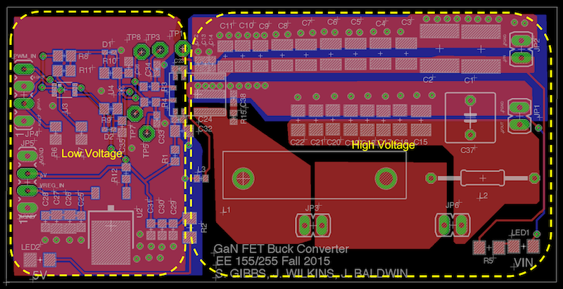
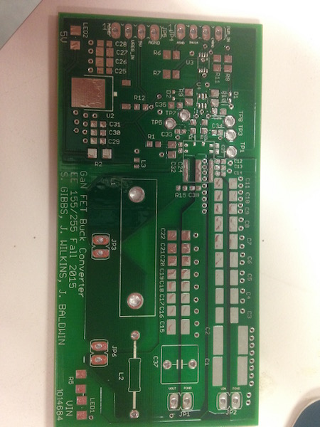
PCB Layout
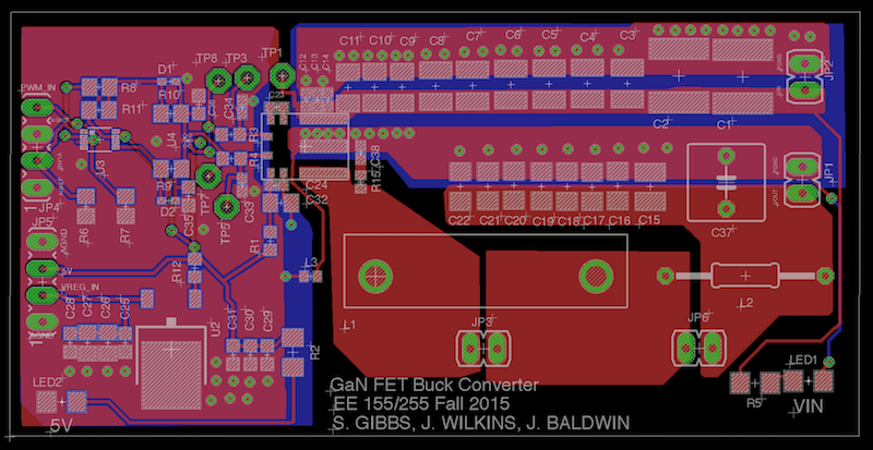
Our PCB layout is shown above. The following images point out specific components. Notice that the power ground and analog grounds are separated in the middle by the ferrite bead an the high and low voltage regions are similarly separated.
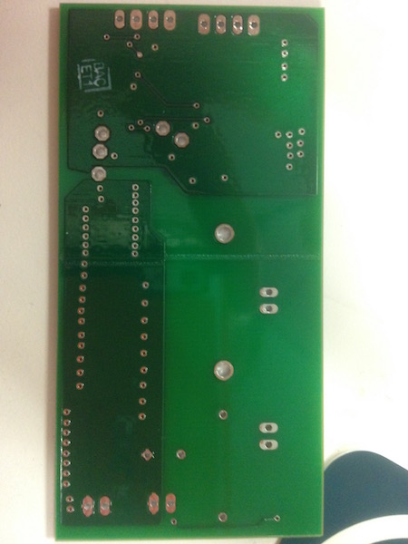
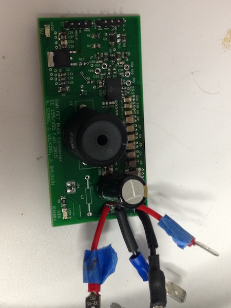
PCB Results
The following images show the final PCB.
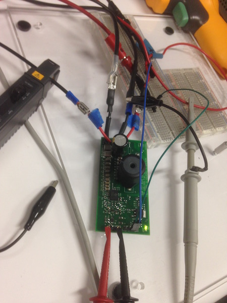
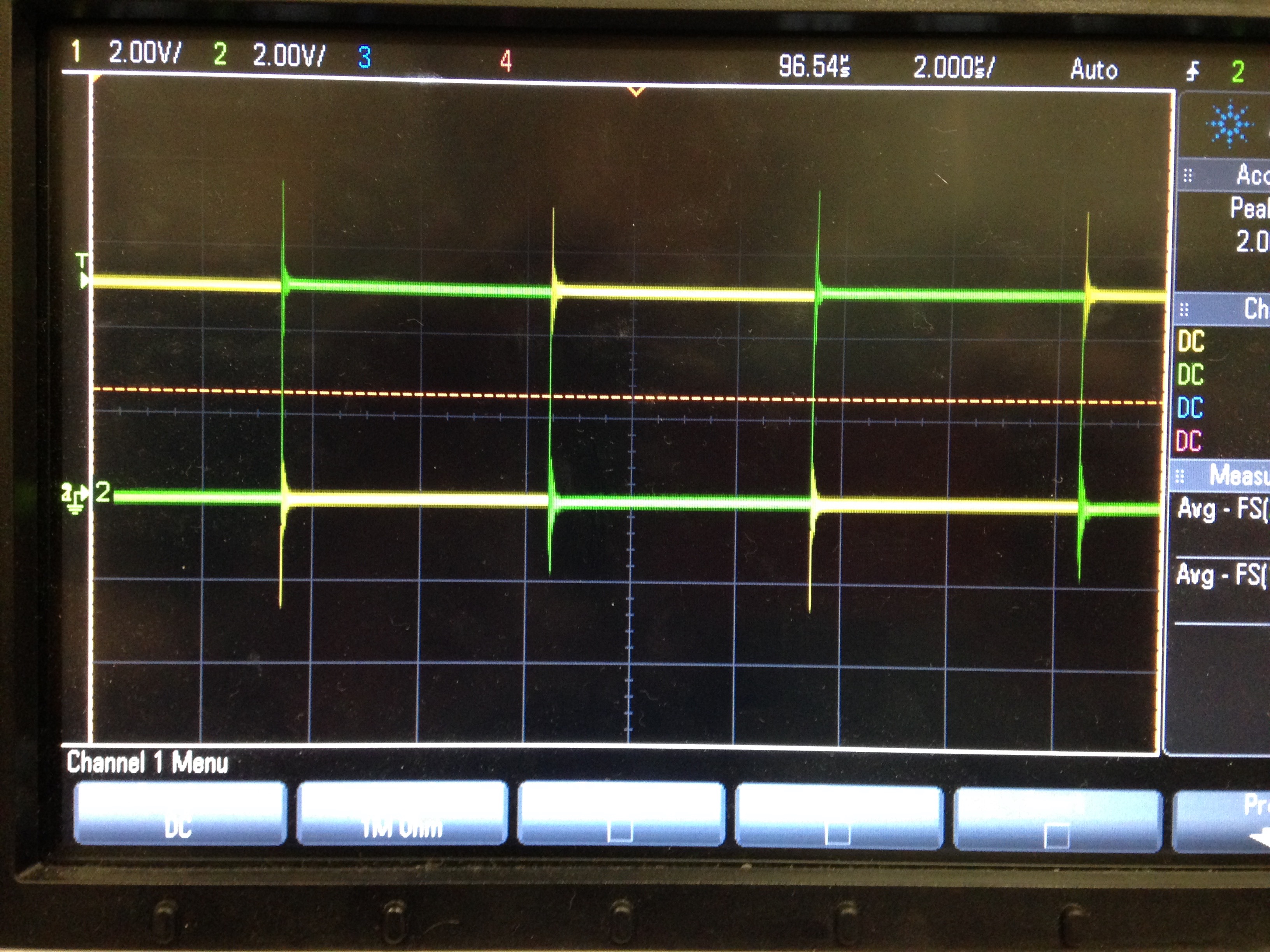
Performance of the Circuit
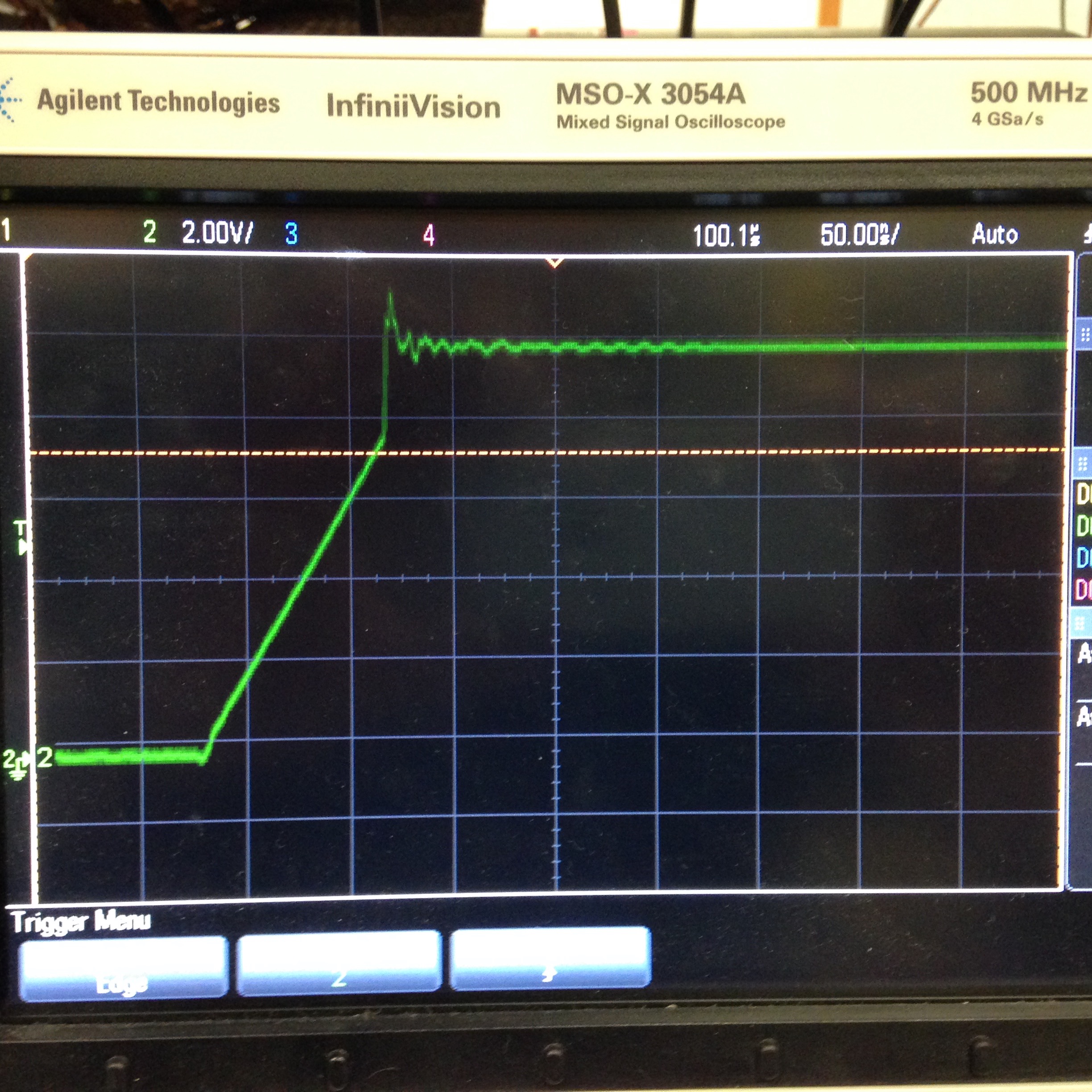
The circuit performed as expected. We input a voltage of 10 V, gave the half-bridge a 50% duty cycle, and the output voltage stayed at approximately 5 V. Below are the measured efficiencies and pictures from the circuit in operation. The efficiencies are slightly inaccurate because we couldn't get a good current reading at the input, but they are close.
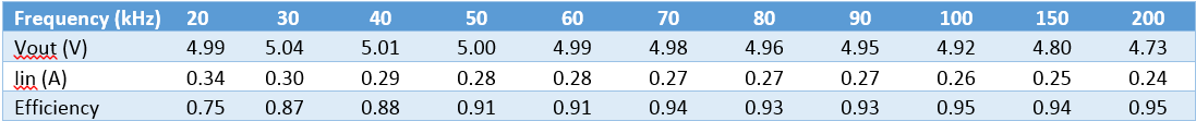

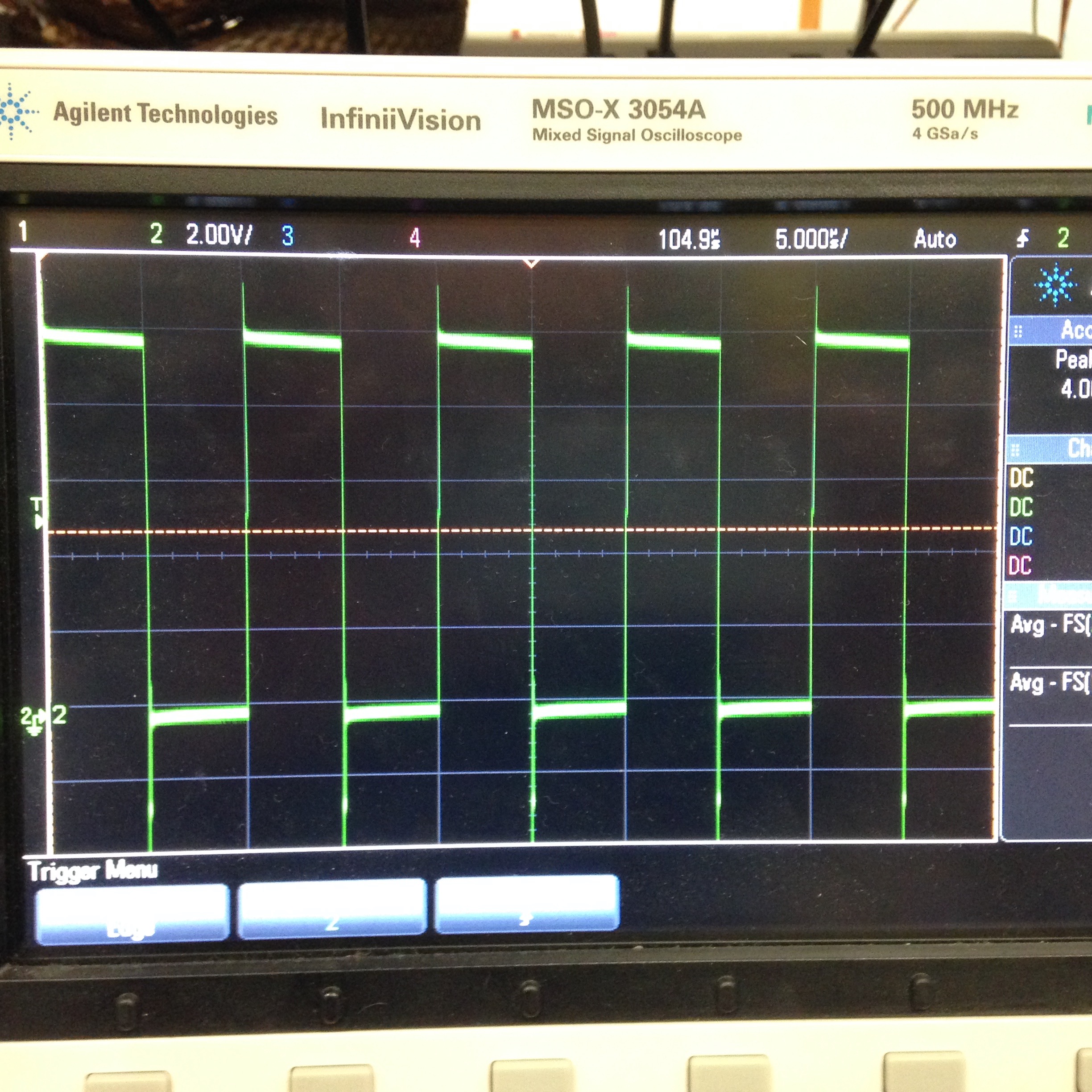
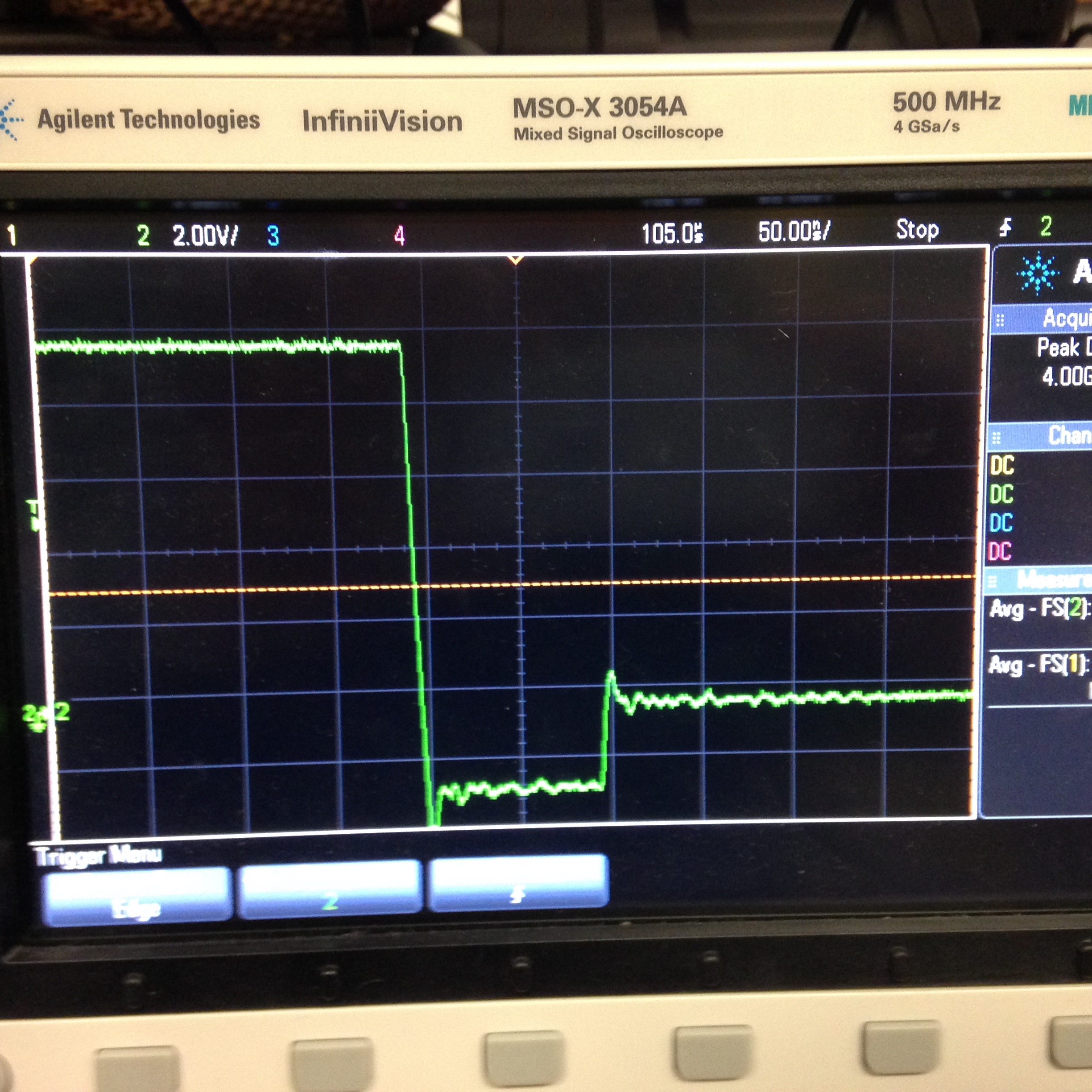
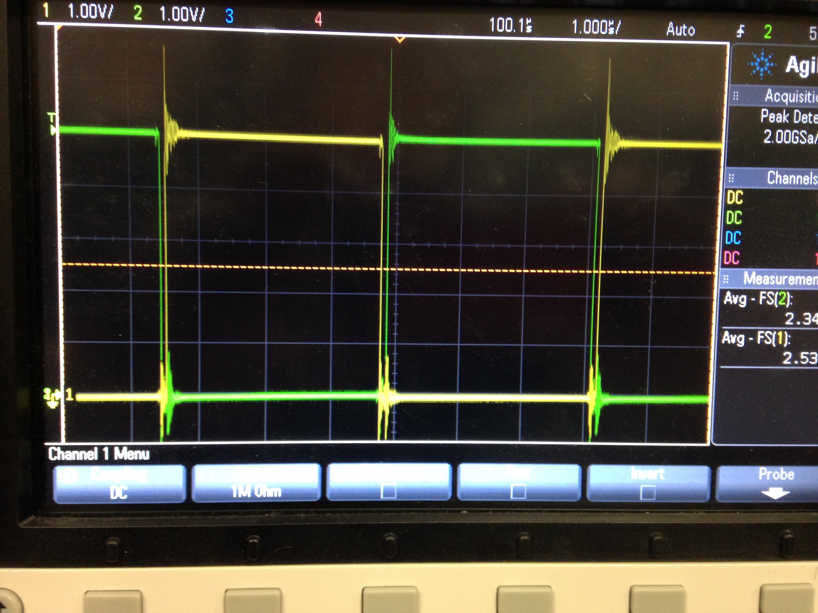
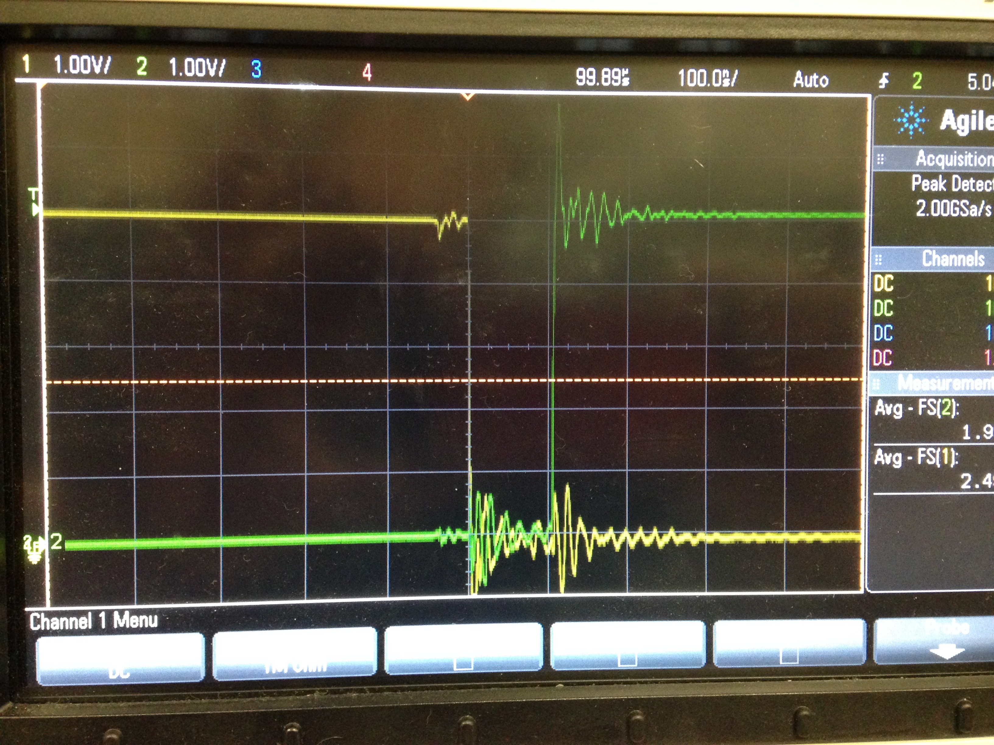
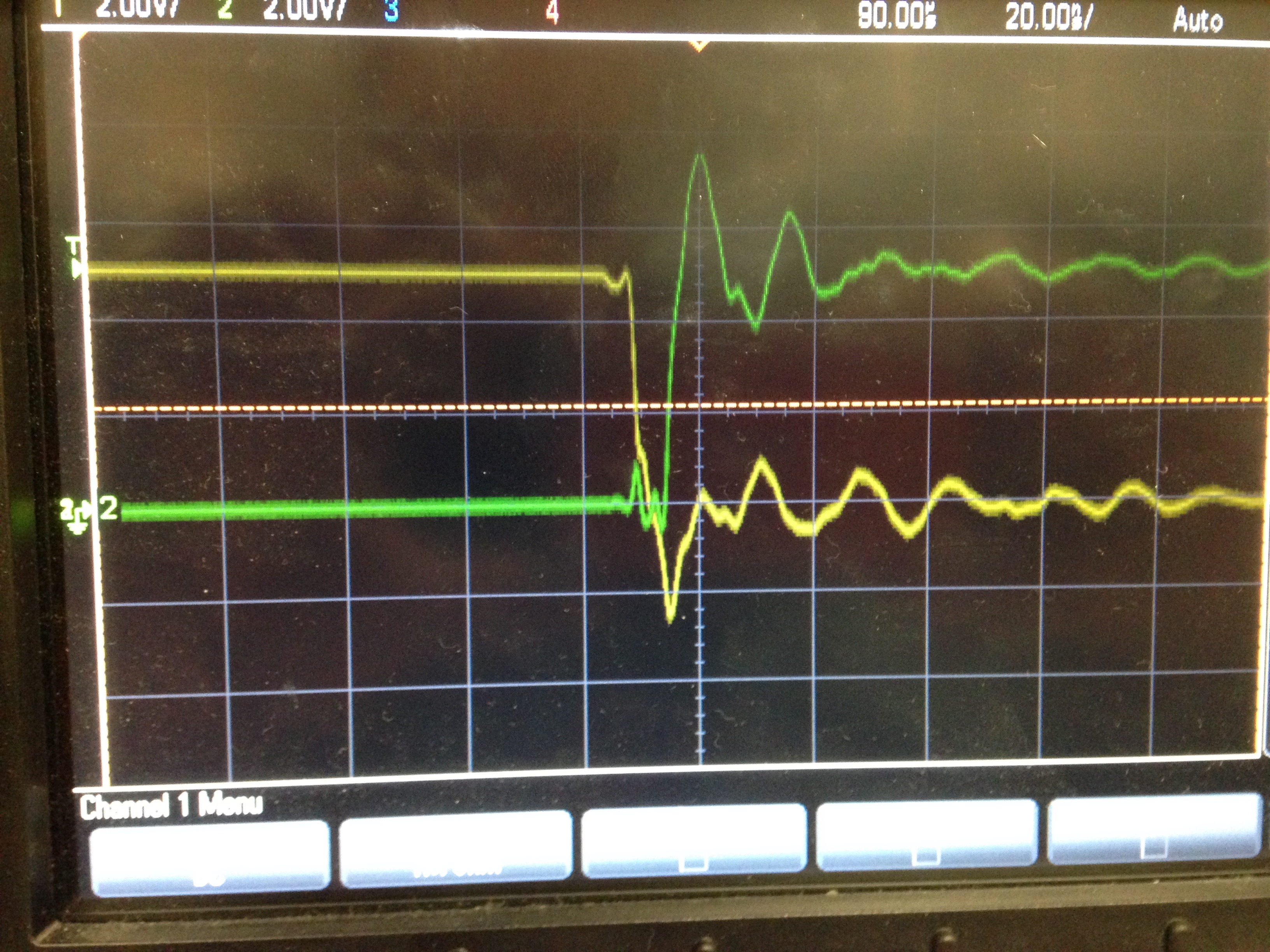
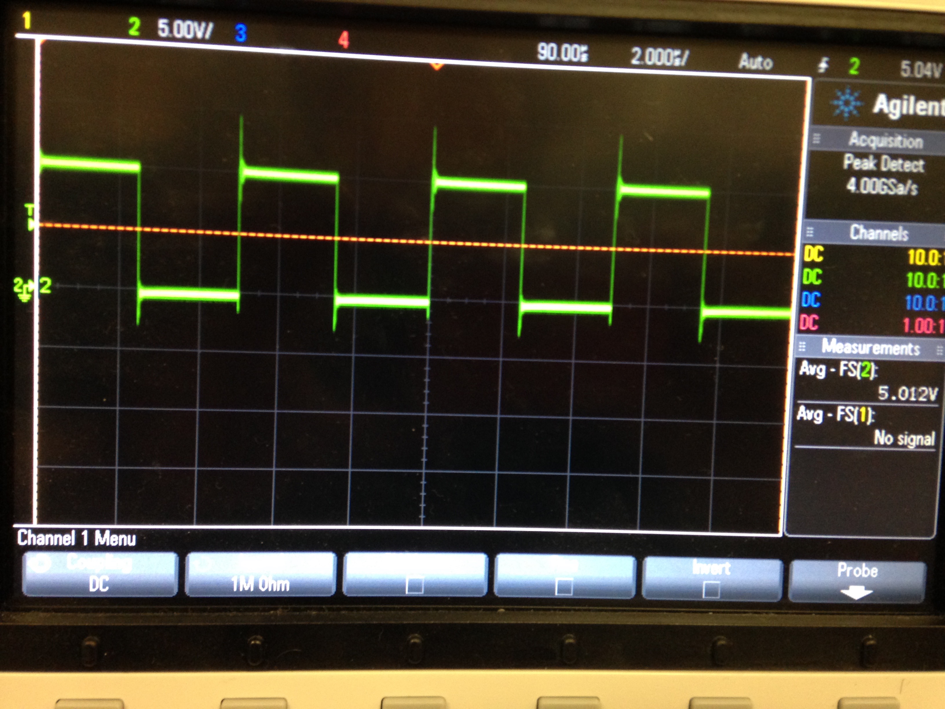
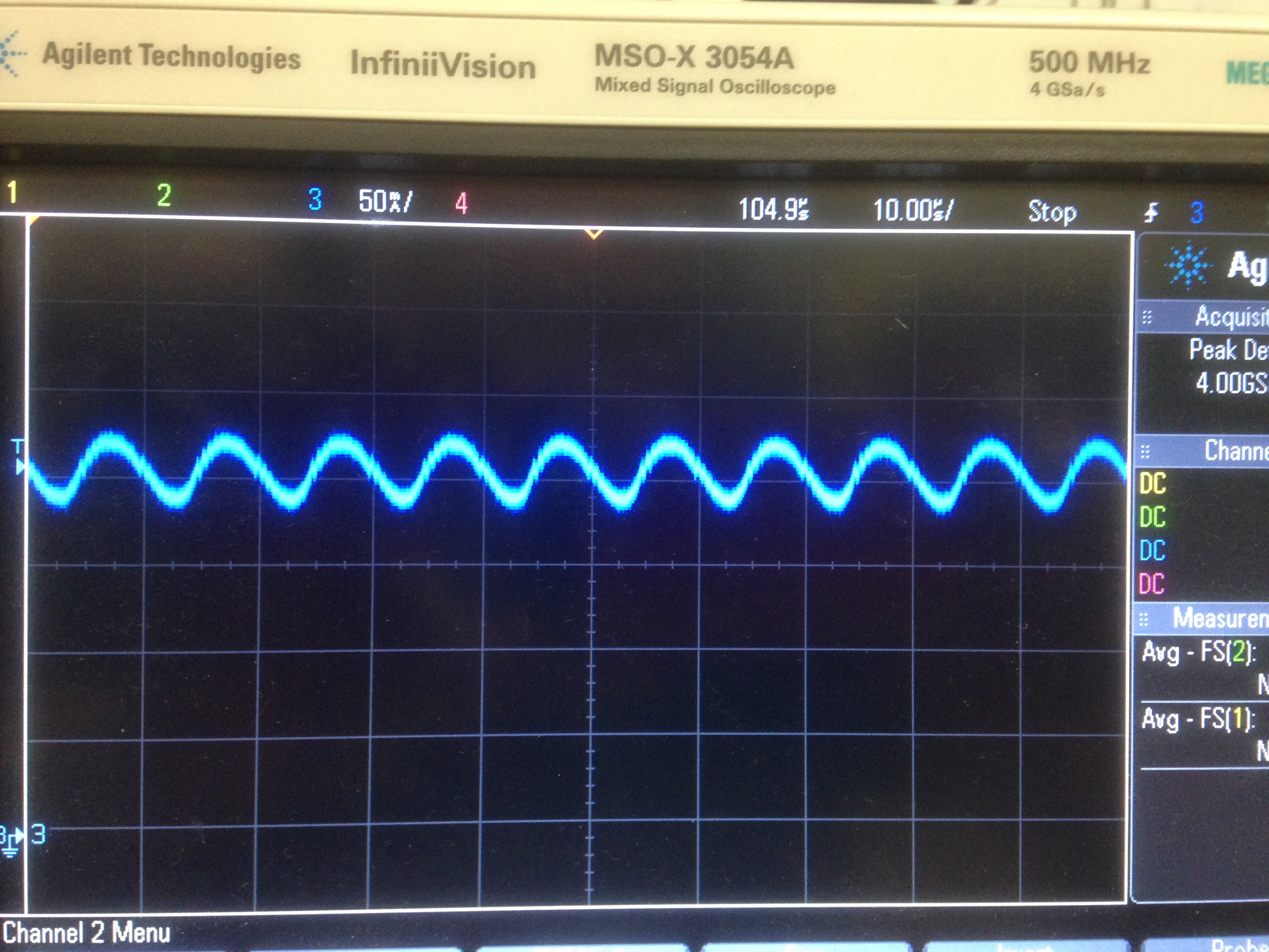
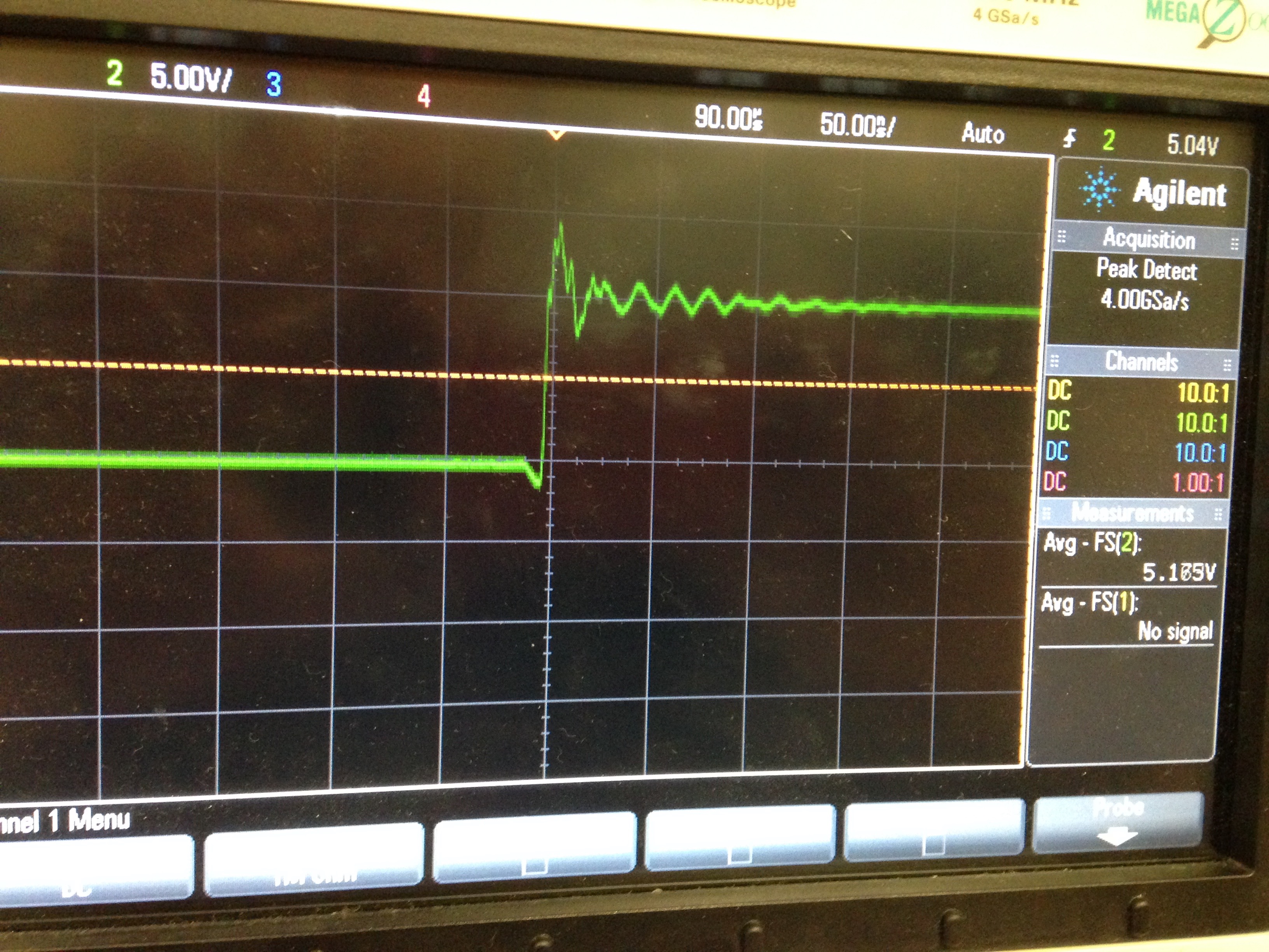
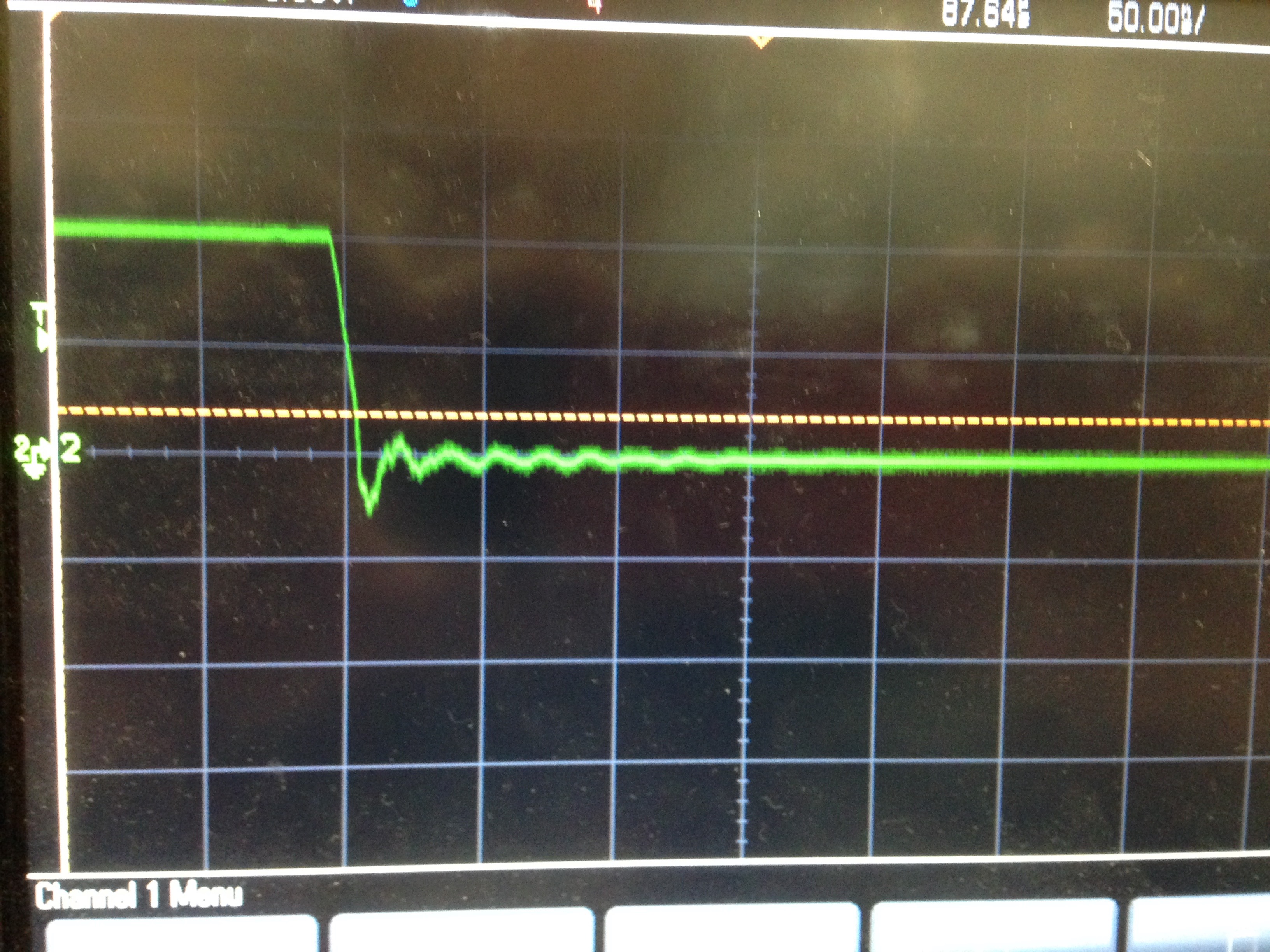
Although there is some ripple and ringing, this behavior was relatively minor and didn't seem to affect overall performance much. The circuit also behaved more or less like the simulation, which is good.
Conclusions and Future Work
In this project we have demonstrated the ability to safely drive a GaN FET half brige in a buck converter configuration with over 97% efficiency. The use of an integrated halfbridge module and careful PCB layout reduced the inductive and capacitive parasitics in the switching loop and on the switching node enough to prevent catastrophic ringing which is a common problem for GaN FET circuits.
There are many directions we could take this in the future. In the interest of time our circuit testing was rather limited. We could continue to play with the deadtime and we could add in components for the snubber. Additionally we could consider trying to eliminate the ringing on the output of the deadtime circuit, and maybe increse the ferrite impedance to see if the noise on the deadtime output is caused by coupling through the grounds.
A great potential application for GaNs is in microinverters for the solar industry. Their efficiency at the voltages encountered in PVs makes them a candidate for reducing inverter cost. It would be interesting to develop inverters based on this new technology and a potential future direction for work.
Thanks
We would first like to thank our great TAs for all their help this quarter. Their dedication and interest in our learning made for a great lab environment and improved learning outcomes. We would also like to thank Professor Dally for his excellent lectures, guidance, and enthusiasm.
References
1. LMG5200 80-V, GaN Half-Bridge Power Stage Data Sheet. Texas Instruments. http://www.ti.com/lit/ds/symlink/lmg5200.pdf.
2. Mehta, Narendra. "SV601148A_HW.SchDoc-001_Schematic." Texas Instruments. http://www.ti.com/lit/zip/snor008. Mar. 2015.