
|

|
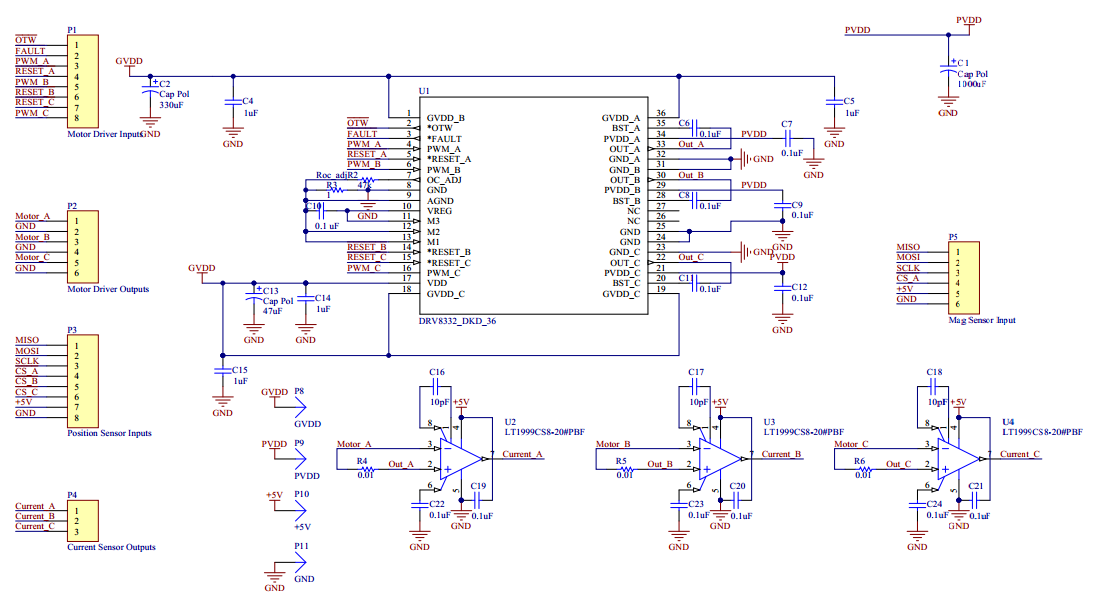
Schematic
Board Design
The top layer includes all connections from the STM32F4 discovery board to the inputs of the DRV8332 chip. High current traces, those that connect to PVDD and output drive pins, are kept as short and wide as possible.
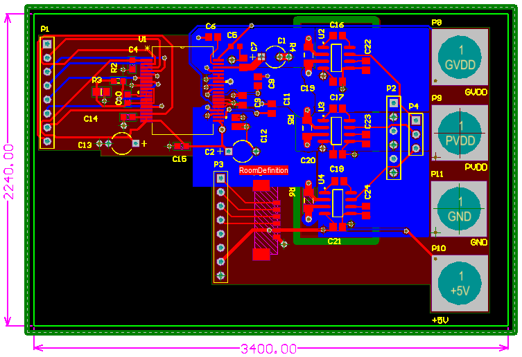
The second layer of the board consists of a split analog-digital ground plane, with the analog plane running underneath the LT1999 current sense chip. This was done to minimize ground noise, and maintain low ground impedance for the analog circuitry. The layout for lowest EMI/noise susceptibility is achieved by keeping short direct connections and keeping the sense resistor close to the LT1999. Reference bypass capacitor on pin 6 is tied to the analog ground. Note that the LT1999 has 100dB of CMRR and therefore do not need a quite ground for input sensing purposes. They do need a bypass cap from power to GND right next to the sensor chip. The only reason to keep the LT1999 GND quiet is that GND noise will be added to the output signal.

The third layer of the board consists of a split power-plane with 5V running underneath the LT1999 current sense chips and PVDD elsewhere. This was done to maximize the PVDD trace width to tolerate high currents while providing easy routing options for the current sense electronics.

The last layer of the board primary consisted of traces for the high-power signal outputs of the DRV8332 motor driver chip. These traces were designed to be polygonal fill areas to handle large currents.

Electronic BOM (excluding PCB board)
| brushless_motor_driver_breakout_board_bom_-_digikey.pdf |
PCB Design Files
| drv8332_motordriver_shield.schdoc |
| drv8332_motordriver_shield.pcbdoc |
Gerber Files
| brushless_motordriver_shield_gerbers.zip |