H.-S. Philip Wong

Professor of
Electrical Engineering
Willard R. and Inez
Kerr Bell Professor in the School of Engineering
Education:
B.Sc. Hons. (1982) University of Hong Kong, M.S. (1983) State University of New York, Stony Brook, and Ph.D. (1988) Lehigh University.
Biography:
H.-S. Philip Wong is the Willard R. and Inez Kerr Bell Professor in the School of Engineering. He joined Stanford University as Professor of Electrical Engineering in September, 2004.
From 1988 to 2004, he was with the IBM T.J. Watson Research Center where he did many of the early research works that have led to product technologies.
From 2018 to 2020, he was on leave from Stanford and was the Vice President of Corporate Research at TSMC, the largest semiconductor foundry in the world, and since 2020, remains the Chief Scientist of TSMC in a consulting, advisory role.
Professor Wong’s research aims to translate discoveries in science into practical technologies. His works have contributed to advancements in nanoscale science and technology, semiconductor technology, solid-state devices, and electronic imaging. His present research covers a broad range of topics including carbon electronics, wireless implantable biosensors, device modeling, brain-inspired computing, solid-state memory, and 3D system integration.
He is a member of the National Academy of Engineering and a Fellow of the IEEE, He received the IEEE Andrew S. Grove Award, the IEEE Technical Field Award to honor individuals for outstanding contributions to solid-state devices and technology, as well as the IEEE Electron Devices Society J.J. Ebers Award, the society’s highest honor to recognize outstanding technical contributions to the field of electron devices that have made a lasting impact.
He received an Honorary Doctorate from the Institut Polytechnique de Grenoble, France, and is an Honorary University Fellow of the University of Hong Kong.
He served as the Editor-in-Chief of the IEEE Transactions on Nanotechnology (2005 – 2006), sub-committee Chair of the ISSCC (2003 – 2004), General Chair of the IEDM (2007), and the Chair of the IEEE Executive Committee of the Symposia of VLSI Technology and Circuits (2014 – 2022).
He has held leadership positions at major multi-university research centers of the National Science Foundation and the Semiconductor Research Corporation. He is founding faculty co-director of the Stanford SystemX Alliance – an industrial affiliate program focused on building systems – and the faculty director of the faculty director of the Stanford Non-Volatile Memory Technology Research Initiative (NMTRI). He served as the Director of the Stanford Nanofabrication Facility – a shared facility for device fabrication on the Stanford campus that serves academic, industrial, and governmental researchers across the U.S. and around the globe.
He is the Principal Investigator of the Microelectronics Commons California-Pacific-Northwest AI Hardware Hub, a consortium of over 60 companies and academic institutions funded by the CHIPS and Science Act. He was a member of the US Department of Commerce Industrial Advisory Committee on microelectronics. He serves on the Executive Committee of the UC Berkeley think tank Technology Competitiveness and Industrial Policy (TCIP) Center.
RESEARCH GROUP:
Nanoelectronics and Nanotechnology
List of current and former students, model and research data
downloads, and news are here: http://nano.stanford.edu
Recent talks on
global media:
35th VLSID: “Reimagining semiconductors for our grandchildren’s world,” https://youtu.be/-oqL3ZZLWv8
DARPA ERI Summit 2020: “The Future is System Integration,” https://youtu.be/cJh7EMWa6J0
DAC 2020: “Semiconductor Technology - A System Perspective,” https://youtu.be/zexC_As261s
HotChips 2019: “What Will the Next Node Offer Us?” https://youtu.be/O5UQ5OGOsnM
MIT MTL Seminar
2018: “The Future of Transistor Integration,” https://www.mtl.mit.edu/seminars/future-transistor-integration
Education video on
nanotechnology:
NSF Science Nation video on carbon nanotube nanosystems (produced by the National Science Foundation)
Carbon nanotube technology (funded by the National Science Foundation)
CNT at Stanford: Long, medium, short (funded by the National Science Foundation)
Some time ago, someone posed this question to me: “What comes after the computer chip?” Having spent most of my career advancing semiconductor technology, which is the physical foundation of the computer chip, I find this question worth thinking about. So I wrote this blog on Slate.
In 2017, I was interviewed by the National Nanotechnology Coordination Office (NNCO) of the White House. I talked about our research in this podcast on nano.gov.
OpEd and Opinion articles on semiconductor technology
leadership
“How We’ll Reach a 1 Trillion Transistor GPU,” IEEE Spectrum, March 28, 2024. https://spectrum.ieee.org/trillion-transistor-gpu
“Let’s Put “Tech” into Military Technology Policy,” Air & Space Forces Magazine, April 3, 2025.
H.-S. P. Wong and J. Plummer, “Implications of Technology Trends in the Semiconductor Industry,” Chapter 2 in “Silicon Triangle – The United States, China, Taiwan, and Global Semiconductor Security,” L. Diamond, J. Ellis Jr., O. Schell eds., Hoover Institution Press, October 2023.
“To Reignite the U.S. Chip Industry, Invite More Chefs into the Kitchen,” Scientific American, June 5, 2023.
“Innovating at Speed and at Scale: A Perspective on Next Generation Infrastructure for Accelerating Semiconductor Technologies,” a white paper, March 7, 2022.
“Semiconductors: The US should be asking how we can lead,” The Hill, December 1, 2021.
Videos on semiconductors:
“The Implications of Technology Trends in the Semiconductor Industry” Hoover Institution YouTube video. September 14, 2023.
“How to develop ever-better computer chips,” episode of Stanford Engineering’s The Future of Everything, May 25, 2022.
“Semiconductors: New Lab-to-Fab Solutions and the Future of Semiconductor Technology,” US State Department Foreign Press Center briefing, April 19, 2022.
RESEARCH AREAS: Nanotechnology,
nanoelectronics, semiconductor technology, solid-state devices, Si CMOS,
solid-state imaging.
21st century information technology (IT) must process,
understand, classify, and organize vast amount of data in real-time. 21st
century applications will be dominated by data-centric computing operating on
Tbytes of active data with little data locality. At the same time,
massively redundant sensor arrays sampling the world around us will give humans
the perception of additional “senses” blurring the boundary between biological,
physical, and cyber worlds. Abundant-data processing, which comprises real-time
big-data analytics and the processing of perceptual data in wearable devices,
clearly demands computation efficiencies well beyond what can be achieved
through business as usual.
The key elements of a scalable, fast, and energy-efficient computation
platform that may provide another 1,000× in computing
performance (energy-execution time product) for future computing workloads are:
massive on-chip memory co-located with highly energy-efficient computation,
enabled by monolithic 3D integration using ultra-dense and fine-grained massive
connectivity. There will be multiple layers of analog and digital memories
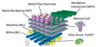
interleaved with computing logic, sensors, and application-specific devices. We call this technology platform N3XT –
Nanoengineered Computing Systems Technology. N3XT will support computing
architectures that embrace sparsity, stochasticity, and device variability.
This technology direction is sometimes called CMOS
+ X, where X can be memory, photonics, spintronics, power electronics,
nanomechanics, sensors and actuators, RF/mm-wave, and even quantum computing.

[N3XT: Nano-engineered Computing Systems Technology. Monolithic 3D integration of memory immersed in logic, connected by ultra-dense vertical connections.]
Going beyond a single monolithic chip, we can put chips into packaged systems as stacked and assembled IC – a concept which we call MOSAIC (Monolithic/Stacked/Assembled IC) that provides a way to build systems that can be scaled up. N3XT 3D MOSAIC provides a continuum of connectivity in the vertical direction from 10s of micrometers to 10s of nanometers, spanning a million times of interconnection density – essentially a completely new interconnectivity continuum (the new IC).
[MOSAIC: Monolithic/Stacked/Assembled IC]
Logic:
For transistors it is important to have an atomically thin channel that enables gate length scaling while maintaining good carrier transport required for a high current drive. At the same time, parasitic resistance from the contacts and parasitic capacitance from the device structure must be minimized. Currently, we are working on the use of carbon nanotube (CNT) and oxide semiconductors (such as indium tin oxide, ITO) as the atomically thin channel. We are also developing techniques to minimize the contact resistance and the parasitic capacitance. By building practical nanosystems of these emerging technologies, we learn how to solve fundamental device and materials science problems that have system-level impact.

[Aligned carbon nanotube growth (Albert Lin, Nishant Patil, Hong-Yu (Henry) Chen, Luckshitha Liyanage)]
[10-nm contact to carbon nanotube (Greg Pitner)]

[A microprocessor made entirely out of carbon nanotubes with > 10,000 CNTs and > 2 billion carbon atoms (Max Shulaker et al.)]
Memory:
I started doing research on memory devices around 2003. Research on memory had been rather “predictable” for many years until recently. It was predictable because the major advances for memory devices involved scaling down the physical dimensions of essentially the same device structure using basically the same materials. The situation has changed in the last two decades. Memory devices are beginning to be difficult to scale down. But perhaps the most important change is that new applications and products (e.g. mobile phones, tablets, enterprise-scale disk storage) in the last decade are often enabled by advances in memory technology, in particular solid-state non-volatile memories.
Our research on memory devices broadly covers phase change memory (PCM), metal oxide resistive switching memory (RRAM), ferroelectric memory and gain cell quasi-non-volatile memory. We aim to understand the fundamental physics of these devices and develop models of how they work. We explore the use of various materials and device structures (e.g. 3D vertical RRAM, amorphous oxide semiconductor for gain cell memory) to achieve desired characteristics. We are working on building memory systems that are monolithically integrated in 3D with logic computing elements.
[RRAM & Gain Cell Integration on Si CMOS (S. Liu et al. in collaboration with CEA LETI)]

[Resistive switching Random Access Memory (RRAM) array (Joon Sohn)]
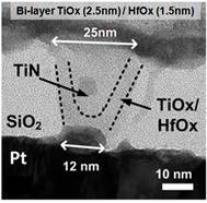

[3D Resistive Switching Random Access Memory (3D RRAM) (Zizhen (Jane) Jiang, Shengjun (Sophia) Qin, Hong-Yu (Henry) Chen, Shimeng Yu, and collaborators at Peking University.)]
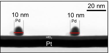
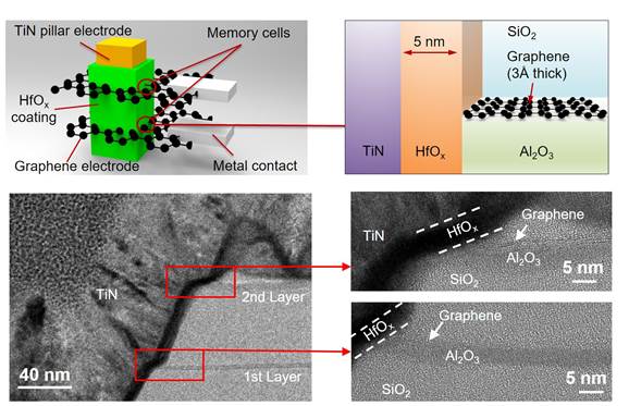
[3D RRAM made with atomically thin (0.3 nm) plane electrode (Joon Sohn, Seunghyun Lee et al.)]
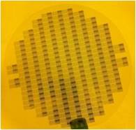
[Nanoscale metal oxide RRAM fabricated by self-assembly patterning (Yi (Alice) Wu, He (Linda) Yi et al.)]
Compute-in-Memory:
We are developing novel memory devices and circuits that implement neural network accelerators on a logic platform that has high-density on-chip non-volatile memories.


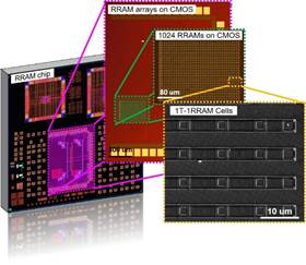
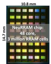
[Compute-in-memory chip with data flow re-configurability. The neurosynaptic core and the full chip with 48 cores and 3 million RRAM cells. W. Wan and UCSD, Tsinghua U, Notre Dame U. collaborators]
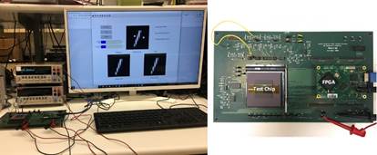
[Demo of image recovery using RRAM compute-in-memory chip (@ISSCC 2020 and @SympVLSI 2020) https://youtu.be/b7ITxmfaLBk]

[SAPIENS chip: One-shot learning and inference at the edge. (Haitong Li, Wei-Chen (Harry) Chen et al.)]

[Hyperdimensional computing using 3D RRAM (Haitong Li and collaborators at UC Berkeley and National Nano Device Laboratory, Taiwan)]
For examples of our works, see
1. W. Wan, R. Kubendran, C. Schaefer, S. B. Eryilmaz, W. Zhang, D. Wu, S. Deiss, P. Raina, H. Qian, B. Gao, S. Joshi, H. Wu, H.-S. P. Wong, G. Cauwenberghs, “A compute-in-memory chip based on resistive random-access memory,” Nature 608, 504–512 (2022)
2. H. Li, W.-C. Chen, A. Levy, C.-H. Wang, H. Wang, P.-H. Chen, W. Wan, H.-S. P. Wong, P. Raina, “One-Shot Learning with Memory-Augmented Neural Networks Using a 64-kbit, 118 GOPS/W RRAM-Based Non-Volatile Associative Memory,” Symp. VLSI Technology, paper T13-4, Kyoto, Japan, June 13 – 19, 2021.
3. W. Wan, R. Kubendran, B. Gao, S. Joshi, P. Raina, H. Wu, G. Cauwenberghs, H.-S. P. Wong, “A Voltage-Mode Sensing Scheme with Differential-Row Weight Mapping For Energy-Efficient RRAM-Based In-Memory Computing,” Symp. VLSI Technology, Honolulu, HI, paper TM2.2, June 15 – 19, 2020.
4. W. Wan, R. Kubendran, S.B. Eryilmaz, W. Zhang, Y. Liao, D. Wu, S. Deiss, B. Gao, P. Raina, S. Joshi, H. Wu, G. Cauwenberghs, H.-S. P. Wong, “A 74 TOPS/W CMOS-RRAM Neurosynaptic Core with Dynamically Reconfigurable Dataflow and In-situ Transposable Weights for Probabilistic Graphical Models,” International Solid State Circuits Conference (ISSCC), paper 33.1, pp. 498 – 499, San Francisco, CA, February 18 – 20, 2020.
5. H. Li, T.F. Wu, A. Rahimi. K.-S. Li, M. Rusch, C.-H. Lin, J.-L. Hsu, M.M. Sabry, S.B. Eryilmaz. J. Sohn, W.-C. Chiu, M.-C. Chen, T.-T. Wu, J.-M. Shieh, W.-K. Yeh, J. M. Rabaey, S. Mitra, and H.-S. P. Wong, “Hyperdimensional Computing with 3D VRRAM In-Memory Kernels: Device-Architecture Co-Design for Energy-Efficient, Error-Resilient Language Recognition,” IEEE International Electron Devices Meeting (IEDM), paper 16.1, December 5 – 7, San Francisco, 2016
CellChips – Electronically programmable synthetic biology:
In-situ detection of chemical changes in human body at the cellular level can bring enormous benefits in diagnosis and in therapeutic monitoring. We are developing techniques to place micron-sized sensor chip inside each cell.
These CellChips will be equipped with molecular sensors and effectors that allow them to sense and trigger different cellular signaling or gene regulatory pathways. Using bi-directional radio communication with the sensor and effector functions, we will be able to change connections between cellular signaling pathways at will, in real time, without the need to generate new genetic constructs. This technology will provide to synthetic biology the same rapid prototyping and reconfigurability that was brought to electronics by field-programmable gate array (FPGA) technology deployed in data centers, and a variety of information and communication technologies that require reconfiguration post-deployment.
This is a fundamentally new way to dynamically alter
cellular signaling pathways, and will open up an array of new biomedical
applications that range from novel medical diagnostic and therapeutic tools
that operate at single cell level to a novel class of autonomously operating
intrabody nanobiosensors and nanoacutators.
Nanofabrication and integrated electronics are the key enabling technologies of this research.

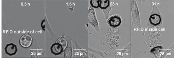
[Uptake of RFID by living cells (Xiaolin (Jasmine) Hu, Mimi Yang, Kokab Parizi)]
Examples of our research can be found in the publications and conference presentations listed below.
PUBLICATIONS: https://scholar.google.com/citations?user=HWxGEesAAAAJ&hl=en
Recent and Upcoming
Invited Presentations:
1.
H.-S. P. Wong, “Beyond
the Exit of the Device Miniaturization Tunnel,” plenary talk, International
Conference on Frontiers of Characterization and Metrology for Nanoelectronics,”
Monterey, CA, USA. March 16 – 19, 2026
2.
H.-S. P. Wong, “Oxide
Semiconductor Gain Cell Memory,” plenary talk, 17th Annual
Non-Volatile Memories Workshop (NVMS), Santa Clara, CA, USA. March 9-10, 2026
3.
H.-S. P. Wong, “AI
Compute Needs Massive and Diverse Memories,” plenary talk, Association for the
Advancement of Artificial Intelligence (AAAI) Spring Symposium, March
31 – April 2, 2025.
4.
S. Liu, R. M. Radway, X. Wang, J. Kwon, C. Trippel,
P. Levis, S. Mitra, H.-S. P.
Wong, “Future of Memory: Massive, Diverse, Tightly Integrated
with Compute – from Device to Software,” International Electron Devices
Meeting (IEDM), paper 3.5, San Francisco, December 2024.
5.
H.-S. P.
Wong, “Design and Design Automation for a Future
Generation of Chips,” invited keynote paper, International Conference on
Computer-Aided Design (ICCAD), Newark,
NJ, October 27-30, 2024.
6.
S. Li, C. Gilardi, G. Zeevi, S.
Mitra, H.-S. P. Wong, “High-Performance Carbon Nanotube Transistors for
Logic Platform,” keynote, 245th ECS Meeting, Symposium on Carbon Nanostructures
and Devices, San Francisco, CA, May 26 - 30, 2024
7.
H.-S. P.
Wong, “Oxide Semiconductor Gain Cell Memory,” invited
keynote paper, 18th International Thin-Film Transistor Conference (ITC 2024),
Daejeon, Korea, March 27 – 29, 2024
Selected Recent and
Upcoming Conference Publications:
1. J. Kang, K.
Jana, N. Safron, D. Zhong, S. Li, H.-S. P. Wong,
"Quantum-Well Carrier Confinement Overcomes Mobility–VT Trade-off of Oxide
Semiconductor Transistors," IEEE International Electron Devices Meeting
(IEDM), paper 22.1, 2025.
2. C.-H. Huang,
K. Jana, S. A. van Rijs, H.-S. P. Wong, "Contact
Length Scaling Enables Suppression of Contact Doping in Oxide Semiconductor
Transistors," IEEE International Electron Devices Meeting (IEDM), paper
22.5, 2025.
3. S. Liu, K.
Jana, L. J.-C. Liu, E. Ambrosi, M. Song, L. Liu, J. Wang, S. Mitra, X. Bao,
M.-F. Chang, J. R. Hu, J. Y. Chen, J. Chen, H.-S. P. Wong, "Amp
Cell: 3D-Scalable Gain Cell Memory with Decoupled Read, Write, and Store,"
IEEE International Electron Devices Meeting (IEDM), paper 28.8, 2025.
4. S. Liu, K.
Jana, L. Liu, J. Wang, L. J.-C. Liu, E. Ambrosi, M. Song, C. Kubicka, Y.
Tan, H. Li, S. Mitra, J. Chen, T. Tambe, X. Bao, M.-F. Chang, J. R. Hu, J. Y.
Chen, H.-S. P. Wong, "Gain Cell Memory Scalability to 5-nm and
Beyond," IEEE International Electron Devices Meeting (IEDM), paper 29.5,
2025.
5. K. Jana, J.
Kang, S. Liu, F. F. Athena, C.-H. Huang, Y. Tang, H.-Y. Chen,
B. Saini, J. Hartanto, R. K. A. Bennett, A. E. O. Persson, S. Li, K.
Neilson, Y.-M. Lee, K. Leitherer, K. Nomura, P. McIntyre, E. Pop and H.-S.
P. Wong, “Key to Low Supply Voltage: Transition Region of Oxide
Semiconductor Transistors,” Symp. VLSI Technology and Circuits, Kyoto,
Japan, paper T17-1, 2025.
6. F. F. Athena,
J. Kang, M. Passlack, N. Safron, D. Dede, K. Jana, B. Saini, X.
Wang, S. Liu, J. Hartanto, E. Boneh, H. J.-Y. Chen,
C.-H. Huang, Q. Lin , D. Zhong, K. Leitherer, P. C. McIntyre, G. Pitner,
I. P. Radu and H.-S. P. Wong, “Orthogonal VT Tuning for Oxide
Semiconductor 2T Gain Cell Enabled by Interface Dipole Engineering,’ Symp.
VLSI Technology and Circuits, Kyoto, Japan, paper T19-1, 2025.
7. Liu, S.,
Radway, R. M., Wang, X., Moro, F., Nodin, J. F., Jana, K., ...
& Wong, H. S. P. (2024, December). Edge Continual Training and
Inference with RRAM-Gain Cell Memory Integrated on Si CMOS. In 2024
IEEE International Electron Devices Meeting (IEDM).
8. Athena, F. F.,
Ambrosi, E., Jana, K., Wu, C. H., Hartanto, J., Lee, Y. M., ... Wong, H. S.
P. & Bao, X. Y. (2024, December). First demonstration of an np oxide
semiconductor complementary gain cell memory. In 2024 IEEE
International Electron Devices Meeting (IEDM).
9. Shuhan Liu, Shengjun
Qin, Koustav Jana, Jian Chen, Kasidit Toprasertpong, H-S
Philip Wong, “First Experimental Demonstration of Hybrid Gain Cell Memory
with Si PMOS and ITO FET for High-speed On-chip Memory,” 2024 IEEE Symposium
on VLSI Technology and Circuits (VLSI Technology and Circuits), Honolulu,
HI, USA, 2024.
Recent Invited
Journal Articles:
1. H.-S. P. Wong, S. Mitra, “Devices, Materials, Process Technologies, and Microelectronic Ecosystem Beyond the Exit of the Device Miniaturization Tunnel, IEEE Trans Materials for Electron Devices, vol. 1, pp. 160-167, 2024, doi: 10.1109/TMAT.2024.3484369. (2024).
2. Aaron D Franklin, Mark C Hersam, H-S Philip Wong, “Carbon nanotube transistors: Making electronics from molecules,” Science, vol. 378, issue 6621, pp. 726 – 732 (2022)
3. C.R. Kagan, T. Hyeon, D.-H. Kim, R. Ruiz, M.C. Tung, H.-S. P. Wong, “Self-assembly for electronics,” invited review, MRS Bulletin, Volume 45, Issue 10 (Functional Materials and Devices by Self-Assembly), October 2020.
4. D. Akinwande, C. Huyghebaert, C.-H. Wang, M. I. Serna, S. Goossens, L.-J. Li, H-S. P. Wong, and F. H. L Koppens. "Graphene and two-dimensional materials for silicon technology," Nature 573, no. 7775 (2019): 507-518.
5. M. D. Bishop, H.-S. P. Wong, S. Mitra, and M. Shulaker, “Monolithic 3-D Integration,” invited review article, IEEE Micro, Nov/Dec, 2019.
6. M. M. S. Aly, T.F. Wu, A. Bartolo, Y. H. Malviya, W. Hwang, G. Hills, I. Markov, M. Wooters, M.M. Shulaker, H.-S. P. Wong, S. Mitra, “The N3XT Approach to Energy-Efficient Abundant-Data Computing,” invited paper, Proceedings of the IEEE, vol. 107, pp. 19 – 48 (2019).
Selected Recent
Journal Articles:
1. F. F. Athena, J. Hartanto, M. Passlack, J. C. Evans, J. Qin, D. Dede, K. Jana, S. Liu, T. Peña, E. Pop, G. Pitner, I. P. Radu, P. C. McIntyre, and H.-S. P. Wong, “Gate-Dielectric Engineering with an Ultrathin Silicon Oxide Interfacial Dipole Layer for Low-Leakage Oxide-Semiconductor Memories,” Nano Letters 2026 26 (10), 3338-3346.
2. X. Wu, L. R. Upton, J. Chen, P. -K. Hsu, S. Yu and H.-S. P. Wong, "Signal Margin, Density, and Scalability of 3-D DRAM: A Comparative Study of Two Bitline Architectures," in IEEE Transactions on Electron Devices, vol. 72, no. 2, pp. 671-677, Feb. 2025, doi: 10.1109/TED.2024.3520074.
3. S. Liu, K. Jana, K. Toprasertpong, J. Chen, Z. Liang, Q. Jiang, S. Wahid, S. Qin, W.-C. Chen, E. Pop, H.-S. P. Wong, “Design Guidelines for Oxide Semiconductor Gain Cell Memory on a Logic Platform,” IEEE Trans. Electron Devices, Vol. 71, Issue 5, pp. 3329 – 3335, May 2024. DOI: 10.1109/TED.2024.3372938
4. K. Akarvardar, H.-S. P. Wong, “Technology Prospects for Data-Intensive Computing,” Proceedings of the IEEE, vol. 111, Issue 1, pp. 92 – 112 (2023).
5. Qing Lin, Carlo Gilardi, Sheng-Kai Su, Zichen Zhang, Edward Chen, Prabhakar Bandaru, Andrew Kummel, Iuliana Radu, Subhasish Mitra, Greg Pitner, H-S Philip Wong, “Band-to-Band Tunneling Leakage Current Characterization and Projection in Carbon Nanotube Transistors,” ACS nano 17 (21), 21083-21092 (2023)
Selected
Publications Prior to Joining Stanford:
1. T. Skotnicki, J. A. Hutchby, T.-J. King, H.-S. P. Wong, F. Beouff, “The Road to the End of CMOS Scaling,” invited paper, IEEE Circuits and Devices Magazine, pp. 16 – 26, 2005.
2. H.-S. P. Wong, “Beyond the Conventional Transistor,” Solid State Electronics, vol. 49, pp. 755 – 762 (2005).
3. J. Kedzierski, M. Ieong, T. Kanarsky, Y. Zhang, H.-S. P. Wong, “Fabrication of Metal Gated FinFETs Through Complete Gate Silicidation with Ni,” IEEE Trans. Electron Devices, vol. 51, No. 12, pp. 2115 – 2120 (2004).
4. H. Shang, K.-L. Lee, P. Kozlowski, C.D’Emic, I. Babich, E. Sikorski, M. Ieong, H.-S. P. Wong, K. Guarini, and W. Haensch, “Self-Aligned n-Channel Germanium MOSFETs with a Thin Ge Oxynitride Gate Dielectric and Tungsten Gate,” IEEE Electron Device Letters, vol. 25, No. 3, pp. 135 – 137 (2004).
5. J. Kedzierski, M. Ieong, E. Nowak, T.S. Kanarsky, Y. Zhang, R. Roy, D. Boyd, D. Fried, H.-S. P. Wong, “Extension and Source/Drain Design for High-Performance FinFET Devices,” IEEE Transactions on Electron Devices, vol. 50, No. 4, pp. 952 – 958, April, 2003.
6. H. Shang, H. Okorn-Schmidt, J. Ott, P. Kozlowski, S. Steen, E.C. Jones, H.-S. P. Wong, W. Haensch, “Electrical Characterization of Germanium p-Channel MOSFETs,” IEEE Electron Device Letters, vol. 24, No. 4, pp. 242-244, April, 2003.
7. H.-S. P. Wong, J.
Appenzeller, V. Derycke, R. Martel, S. Wind, Ph. Avouris, “Carbon Nanotube
Field Effect Transistors – Fabrication, Device Physics, and Circuit
Implications”, IEEE International Solid State Circuits Conference (ISSCC), p.
370 – 371, 2003.
8. H.-S. P. Wong, “Beyond the Conventional Transistor”, invited paper, IBM J. Research & Development, March/May, pp. 133-168, 2002.
9. J. Kedzierski, E. Nowak, Thomas Kanarsky, Y. Zhang, D. Boyd, R. Carruthers, C. Cabral, R. Amos, C. Lavoie, R. Roy, J. Newbury, E. Sullivan, J. Benedict, P. Saunders, K. Wong, D. Canaperi, M. Krishnan, K.-L. Lee, B. A. Rainey, D. Fried, P. Cottrell, H.-S. P. Wong, M. Ieong, W. Haensch, “Metal-gate FinFET and fully-depleted SOI devices using total gate silicidation”, IEEE International Electron Devices Meeting (IEDM), San Francisco, CA, pp. 247 – 250, 2002
10. L.J. Huang, J.O.Chu, S. Goma, C.P. D’Emic, S. J. Koester, D. F. Canaperi, P. M. Mooney, S. A. Cordes, J. L. Speidell, R. M. Anderson, H.-S. P. Wong, “Electron and Hole Mobility Enhancement in Strained Silicon-On-Insulator by Wafer Bonding,” IEEE Trans. Electron Devices, Vol. 49, pp. 1566 – 1571, September, 2002.
11. B. Doris, M. Ieong, T. Kanarsky, Y. Zhang, R.A. Roy, O. Dokumaci, F.-F. Jamin, L. Shi , W. Natzle, H.-J. Huang, J. Mezzapelle, A. Mocuta, M. Gribelyuk , E.C. Jones, R.J. Miller, H.-S. P. Wong, and W. Haensch, “Extreme Scaling With Ultra-Thin Silicon Channel MOSFET’s (XFET)”, IEEE International Electron Devices Meeting (IEDM), San Francisco, CA, pp. 267 – 270, 2002.
12. K. Rim, E.P. Gusev, C. D’Emic, T. Kanarsky, H. Chen, J. Chu, J. Ott, K. Chan, D. Boyd, V. Mazzeo, B.H. Lee, A. Mocuta, J. Welser, S.L. Cohen, M. Ieong, and H.-S. P. Wong, “Mobility Enhancement in Strained Si NMOSFETs with HfO2 Gate Dielectrics”, Symp. VLSI Technology, pp. 12-13, June, 2002.
13. R. Martel, H.-S. P. Wong, K. Chan, and Ph. Avouris, “Carbon Nanotube Field Effect Transistors for Logic Applications”, IEEE International Electron Devices Meeting (IEDM), Washington, D.C., pp. 159-162, 2001.
14. D.J. Frank, R. H. Dennard, E. J. Nowak, P.M. Solomon, Y. Taur, H.-S. P. Wong, “Device Scaling Limits of Si MOSFETs and Their Application Dependencies”, invited paper, IEEE Proceedings, Special Issue on The Limits of Semiconductor Technology, pp. 259-288, March, 2001.
15. H.-S. P. Wong, D.J. Frank, P.M. Solomon, H.-J. Wann, J. Welser, “Nanoscale CMOS'', IEEE Proceedings, invited paper, Special Issue on Quantum Devices and Applications, pp. 537-570, April, 1999.
Book:
H.-S. P. Wong and D. Akinwande, “Carbon Nanotube and Graphene Device Physics,” Cambridge University Press, 2011. (ISBN-13: 9780521519052). Available at Amazon.com.

CLASSES:
· EE 21N Freshman Seminar (new class since Autumn, 2006, next offering: Spring 2026) – “Making at the nanometer scale: a journey into microchips”).
· EE 309A/B (new class since Autumn, 2020/Winter 2021 (There is no required textbook for this course) – Prerequisite: EE 216. Preferred: EE 271, EE 316, EE 313, EE 311 (with Prof. Priyanka Raina), offered every other year.
· EE 316 (Winter) “Advanced VLSI Devices” offered every other year.
· EE 320 (evolved from EE 218, new in 2008/09) “Nanoelectronics” (There is no required textbook for this course) – Prerequisite EE222, EE216 and knowledge of solid state physics. Recommended: EE 223, 228, or 316.
· (slides for 1st lecture of EE 218 back in Autumn 2005) (rather old, kept here for historical reasons, as a time capsule)
· EE 392B (Spring, 2005, not offered in the near future) “Introduction to Image Sensors and Digital Cameras” (with Prof. Abbas El Gamal)
EE 310 Seminar
slides:
October 5, 2004. Download here. (rather old, kept here for historical reasons, as a time capsule)
Contacts:
H.-S. Philip Wong
Department of Electrical Engineering and Stanford SystemX Alliance,
Paul G. Allen 312X
420 Via Palou,
Email: hspwong AT stanford DOT edu
Phone: +1-650-725-0982
Administrative Assistant: Isabelle London
Email: ilondon AT Stanford DOT edu
Phone: +1-650-724-7833
Directions to campus office and parking information: https://nano.stanford.edu/contact-us
Last modified:
April 14, 2026