Spectral Tweezers: Single Sample Analysis
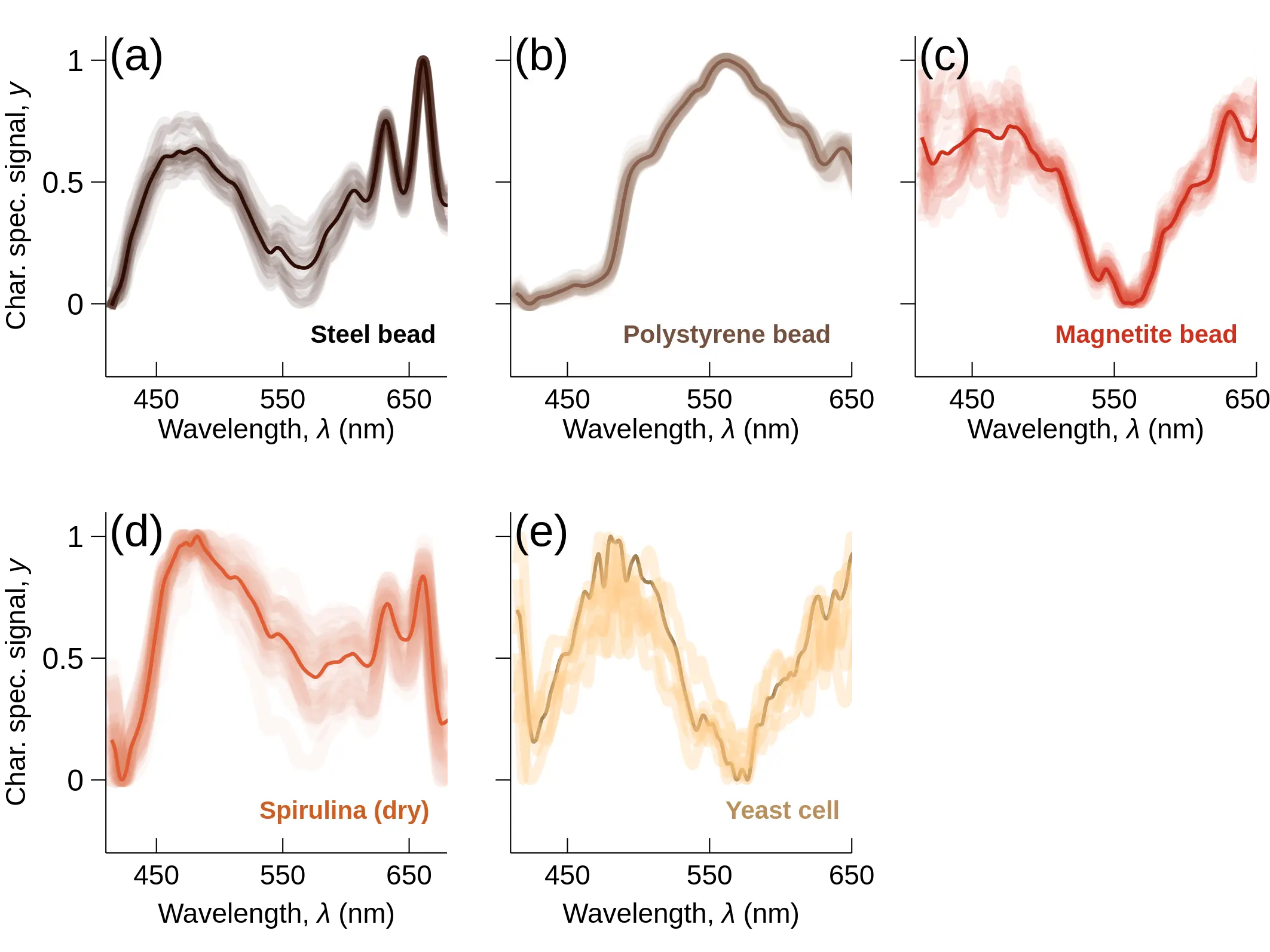
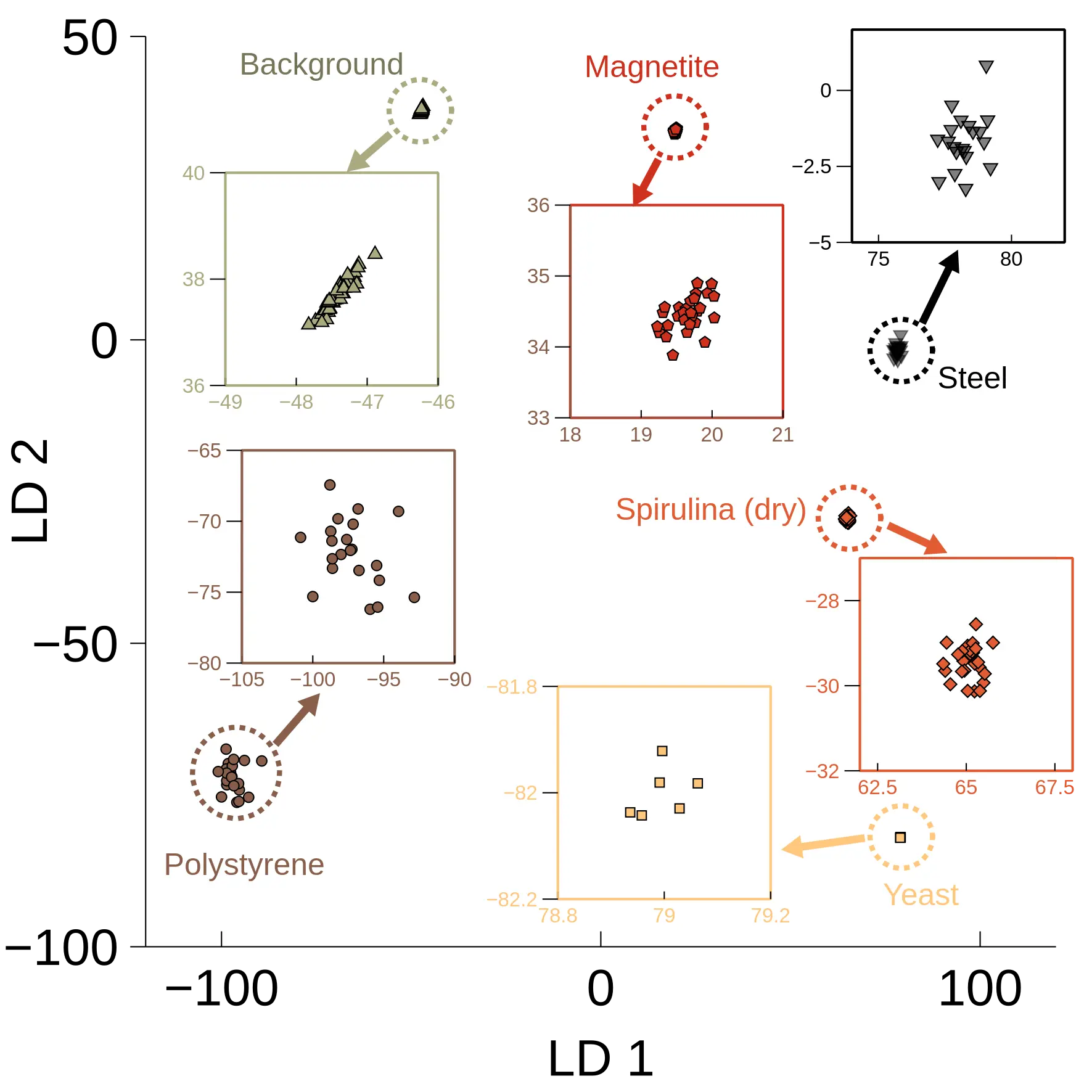
Various types of micro-samples are analyzed using the spectral tweezers setup. Each type of sample is found to exhibits a unique spectral signature. Linear discriminant analysis (LDA) shows that the data points for various sample types do not overlap in the projected reduced dimensional data space and thus can be classified.
The spectral tweezers setup can be implemented using only minor modifications to existing optical microscopes. Only a few off-the-shelf components are needed.
Related Publication(s):
1. Applied Physics Letters: https://doi.org/10.1063/5.0191871
Plasmonic Tweezers with Dynamic Control
Plasmonic tweezers are with a nano C-shaped engraving (CSE) on gold film as the focusing structure is investigated. The CSE is excited using a Nd:YAG laser. The optical response of the structure is polarization dependent. Hence, by controlling the polarization of the incident light (using a half-wave plate), it is possible to adjust the field intensity enhancement near the CSE. Adjusting the field enhancement translates into control over the gradient force. Thus, dynamically controllable plasmonic tweezers can be implemented.
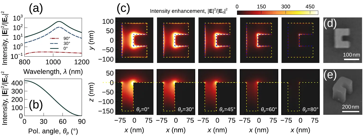
This dynamic control allows one to initially exert large forces to trap a sample while having the capability to reduce the field when the sample is already trapped. Hence, the probability of thermally damaging a trapped sample can be reduced without sacrificing trapping range of the tweezers.
The figures show a schematic representation of CSE, numerical simulation of optical field intensity enhancement near the CSE as a function of polarization angle, and SEM images of patterned photoresist during fabrication. The video shows the trapping of a polystyrene nanoparticle (suspended in water) by a CSE as polarization is varied.
Related Publication(s):
1. Applied Physics Letters: https://doi.org/10.1063/5.0123268
2. Plasmoncis: https://doi.org/10.1007/s11468-022-01735-3
Dielectrophoretic Particle Transport
Dielectrophoresis (DEP) has been widely used for in lab-on-a-chip devices. However, most of these appliations usually handle a large number of samples simultaneously. Achieving control over the DEP force for single particle trapping and controlled transport can be challenging. We used specially designed micro-electrodes and a moving DEP force technique to transport individual microparticles.
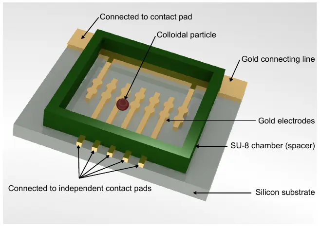
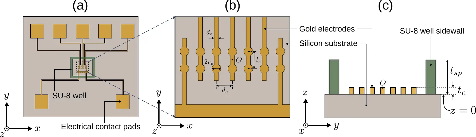
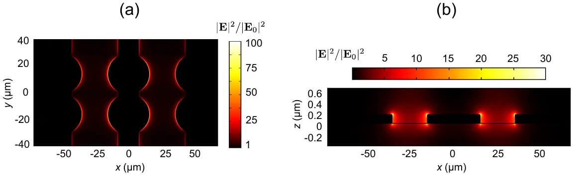
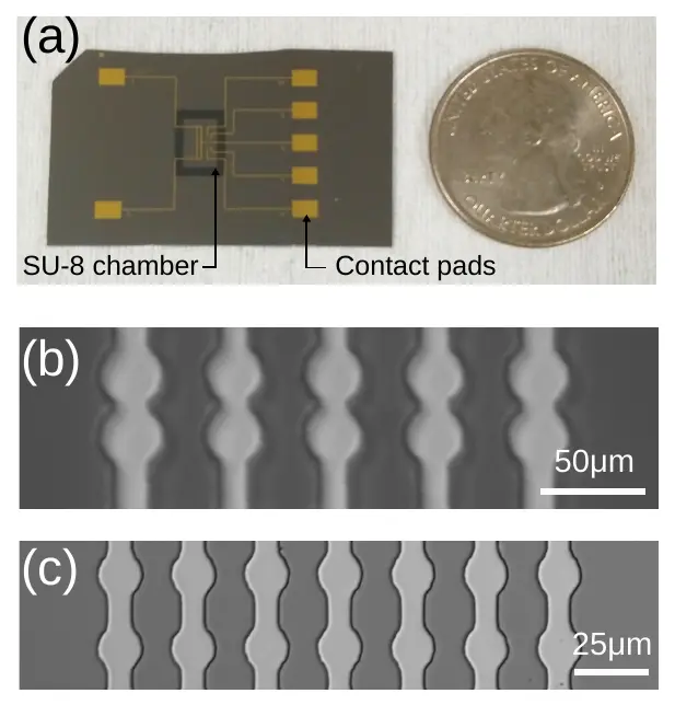
The electrodes are characterized by two circular protrusions. This creates an asymmetry along the y axis; thus producing a confining force in that direction. The electrodes are excited in sequence to create a moving DEP force along the +/- x direction. The overall effect is the creating of a narrow corridor where a propelling force is created. This confinement along with the propulsion force allows us to achieve resolution to transport individual microparticles in a controlled manner.
The figures show a schematic representation of DEP device, numerical simulation of electric field intensity, and images of the fabricated device. The video shows the controlled transport of a polystyrene bead (suspended in water) of diameter 10 micrometer. Overall bidirection transport distance of 1100 micrometer was achieved.
Related Publication(s):
1. Langmuir: https://doi.org/10.1021/acs.langmuir.2c02235
2. Journal of Applied Physics: https://doi.org/10.1063/5.0049126
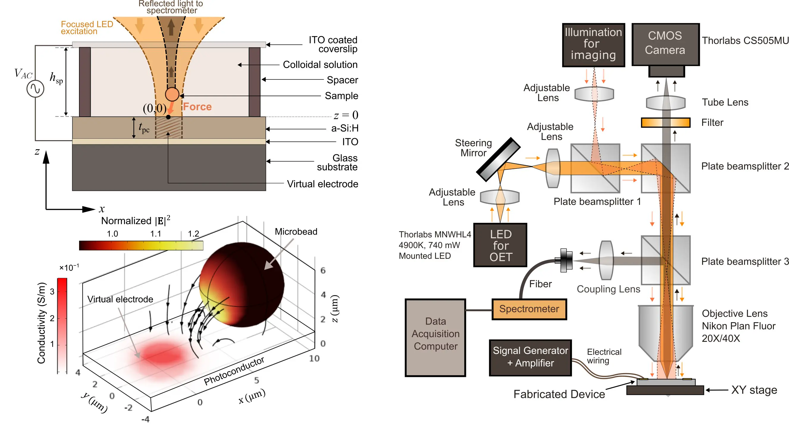
Optoelectronic Tweezers with Nonuniform Background Field
Optoelectronic tweezers (OET) use focused light patterns on a photoconductive material to create "virtual electrodes". When AC voltage is applied between the virtual electrode and a reference electrode, dielectrophoretic forces can be generated to trap and manipulate microparticles. By controlling the light pattern, it is possible to shift the position of the virtual electrode(s), giving the platform flexibility.
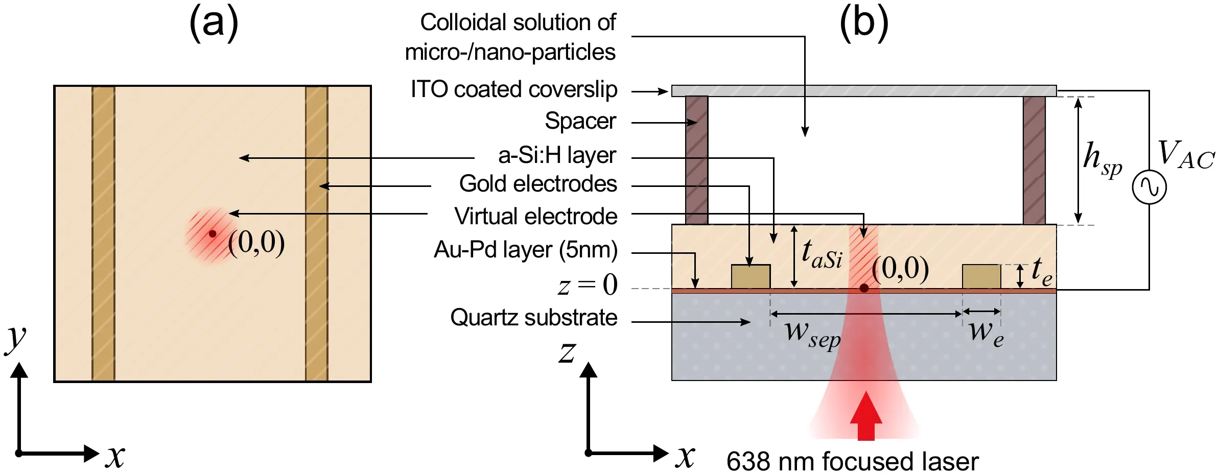
We modify conventional OET design by incorporating a pair of physical gold electrodes below the photoconductor layer. These electrodes produce a non-uniform background field which in turn generates additional gradient forces in the direction perpendicular to their orientation. Thus, the particles can be trapped along a specific axis of the light pattern. This effectively increases the resolution of the OET for a given spot size.
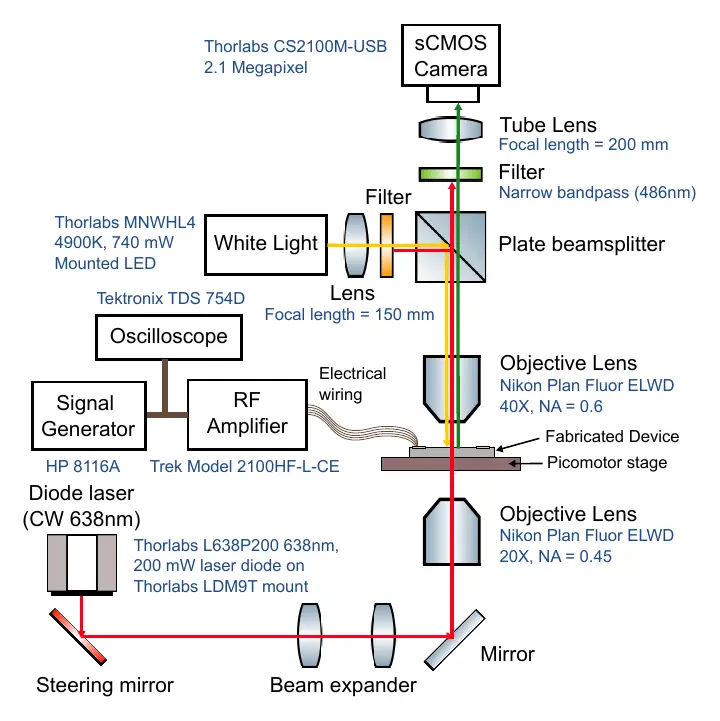
The figures show a schematic representation of OET device, and the experimental setup. The video shows the trapping and manipulation of a polystyrene bead (suspended in water) of diameter 1 micrometer.
Related Publication(s):
1. Applied Physics Letters: https://doi.org/10.1063/5.0020446
Plasmonic Archimedean Spiral
Archimedean spiral shaped plasmonic structures are sensetive to the handedness of circular polarization light. We investigate the optical response of a three turn right-handed plasmonic spiral.
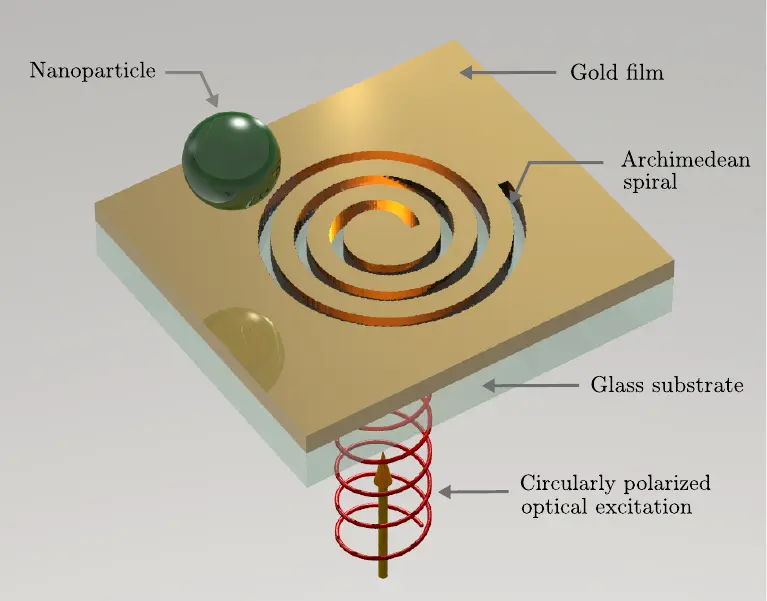
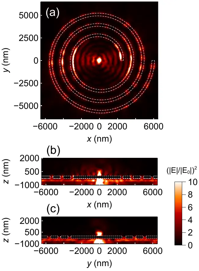
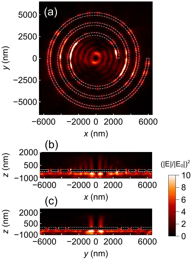
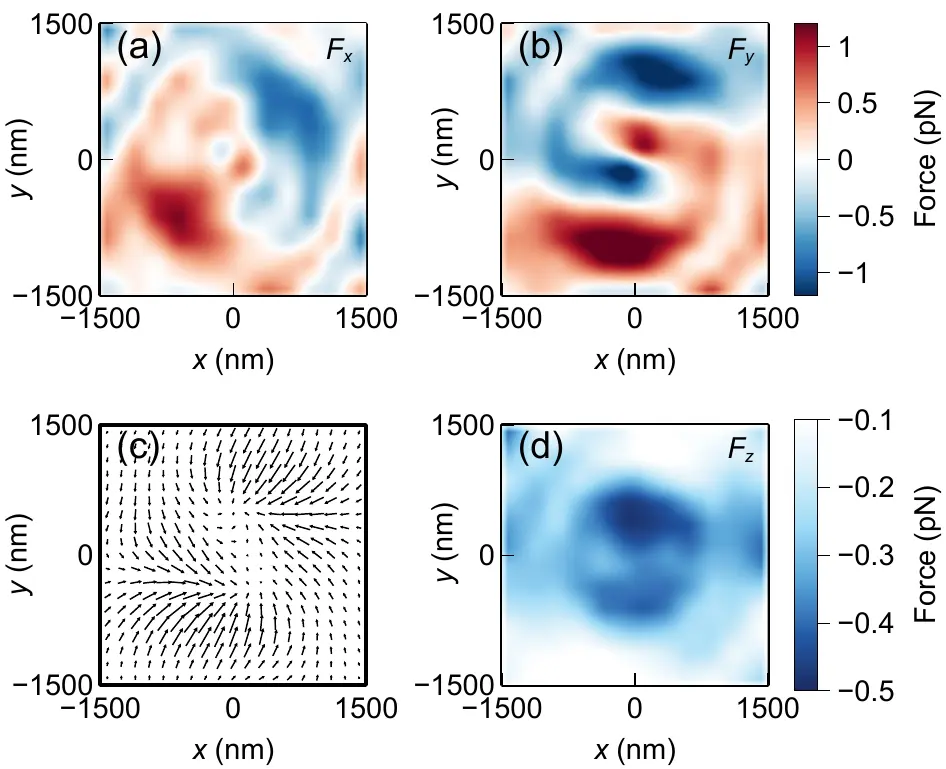
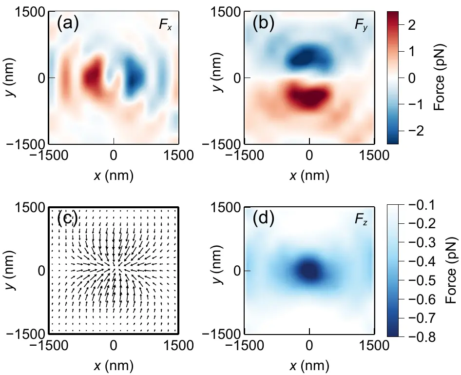
When left-hand-circularly-polarized (LHCP) is incident on the structure at resonance wavelength, the light is focused to a spot. This can produce sufficient optical forces for optical trapping. On the other hand, when right-hand-circularly-polarized (RHCP) light is incident on the structure at resonance wavelength, the light is focused around an annular region. Analyzing the generated force using Helmholtz-Hodge decomposition, the presence of a significant amount of solenoidal force can be identified. Thus, RHCP excitation can produce a force that rotates a trapped particle.
The figures show a schematic representation of the trapping scheme, numerical simulation of optical field intensity enhancement , and calculated force profiles for LHCP and RHCP (the LHCP figures are on the left and the RHCP figures are on the right).
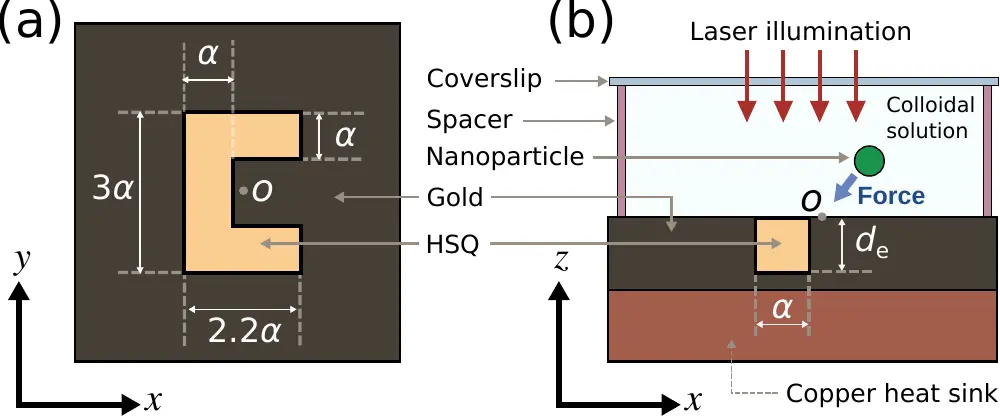
Near-field optical trapping of nanoparticles
Near-field optical trapping schemes use tightly focuses evanescent fields to trap nanoparticles. As evanescent fields can be focused beyond the diffraction limit, such schemes can trap nanoparticles smaller than what a conventional optical tweezers can trap. Plasmonic nano-structures can be used for near-field trapping. We use a C-shaped engraving (CSE) on a gold film as the plasmonic structure.
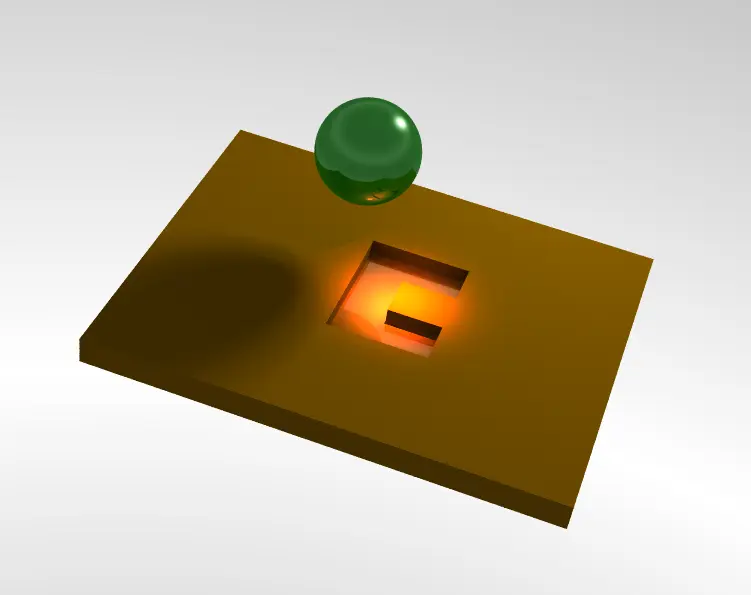
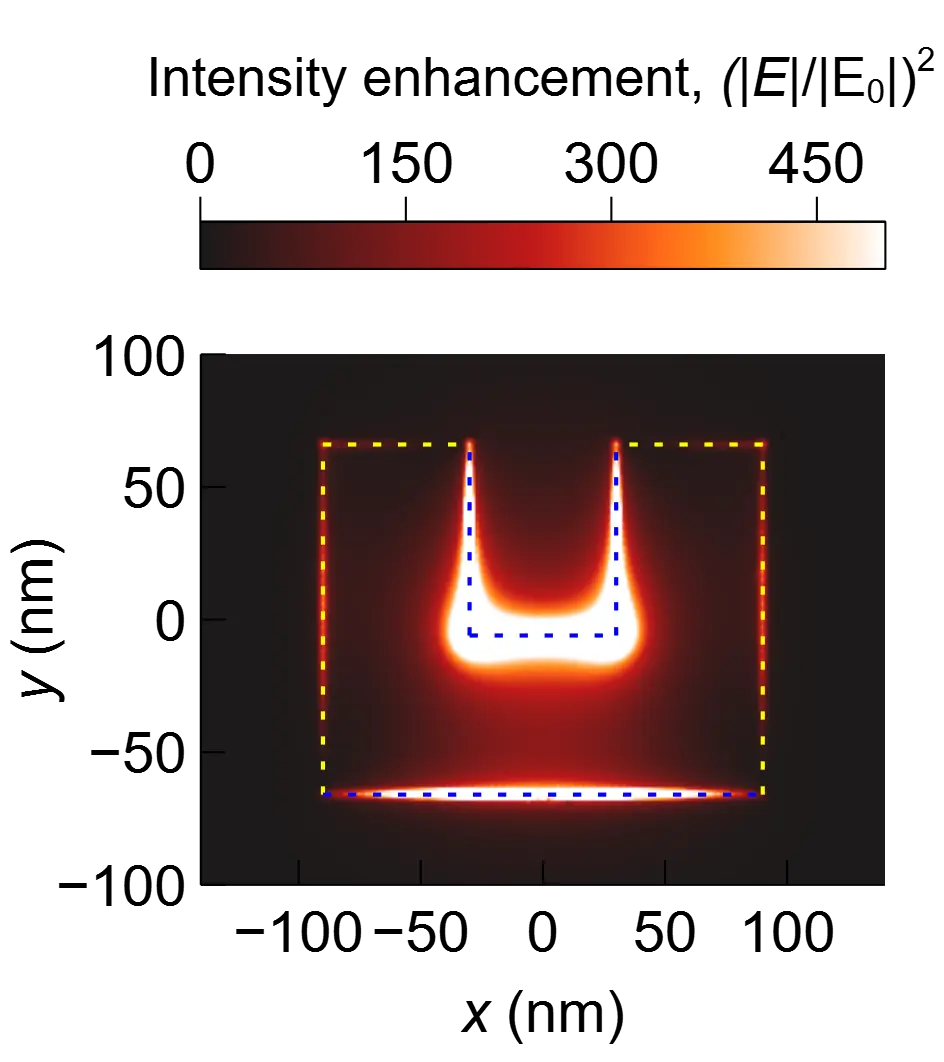
At 1064 nm excitation, the CSE exhibits strong localized field enhancement. As a result, it exerts significant gradient forces that can trap nanoparticles as small as 200 nm in diameter. The force generated by the CSE is non-conservative in nature which can be analyzed using Helmholtz-Hodge decomposition.
The figures show a schematic representation of the trapping scheme, numerical simulation of optical field intensity enhancement near the CSE, and schematic of the experimental setup. The video shows the trapping of a polystyrene nanoparticle (suspended in water) by a CSE. When the nanoparticle is trapped, its Brownian motion decreases significantly.

Related Publication(s):
1. Scientific Reports: https://doi.org/10.1038/s41598-018-36653-0
2. Applied Physics Letters: https://doi.org/10.1063/1.5016810
3. Scientific Reports: https://doi.org/10.1038/s41598-019-45609-x
Dielectrophoresis assisted plasmonic trapping
Near-field optical forces have short range. Due to the strong localized field-intensity enhancement, they can trap very small nanoparticles. On the other hand, dielectrophoretic (DEP) forces have much longer range, but the electromagnetic field spans a larger spot size. Thus dielectrophoretic traps lack the resolution/stiffness of near-field traps. However, using both dielectrophoretic and near-field optical forces, the shortcomings of both schemes can be rectified.
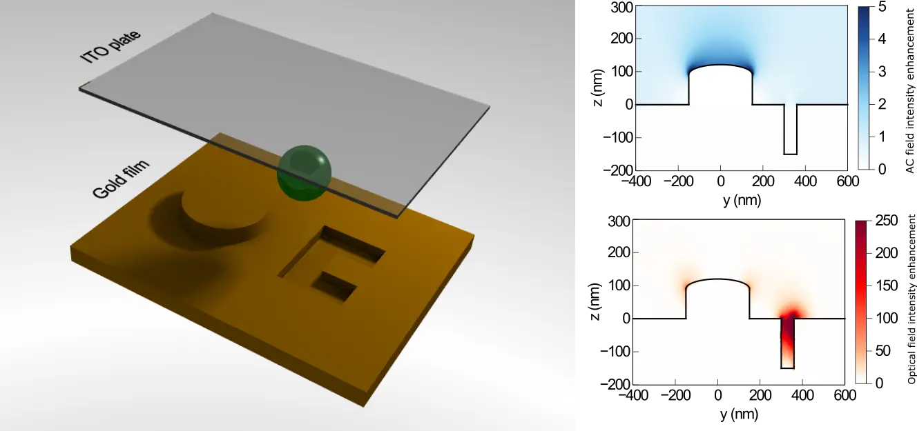
We use a nano-pillar near a C-shaped engraving (CSE). The nano-pillar and an ITO plate act as the electrodes to generate the DEP forces. The long range DEP force can pull-in a nanoparticle from a distance. Once nearby, the optical force from the CSE can take over and the nanoparticle can be transferred to the tighter/stiffer near-field trap.
The figures show a schematic representation of the trapping scheme, numerical simulations of the optical (at 1064 nm) and the AC (at 10kHz) field intensity enhancements.
Related Publication(s):
1. Physical Review A: https://doi.org/10.1103/PhysRevA.95.023840
2. Physical Review A: https://doi.org/10.1103/PhysRevA.96.043825
Adjoint optimization for hysteresis modeling
Adjoint method is a computationally efficient approach of calculating system sensitivity to parameter variation. This technique can be used to calculate the slopes for gradient descent optimization algorithms. This method is used to estimate the parameters of the Jiles-Atherton (JA) hysteresis model.
The JA model can accurately describe the hysteresis behavior of a material once the parameters of the model are identified. The identification process consists of finding the parameter values that best reproduces an experimental hysteresis curve. An optimization algorithm is usually used for this. We show that the adjoint approach gives accurate results with less computational cost than the other approaches.
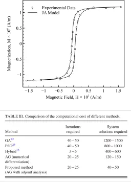
The figure shows comparison between experimental values and the identified JA model. The table shows the comparison of the computational costs.
Related Publication(s):
1. Journal of Applied Physics: https://doi.org/10.1063/1.4962153