After running into several issues with losses, we determined that the amount of dead time used when switching had to be increased. Given that the rise time of the gate drive voltage pulses was 25ns, the dead time was configured so that the switches were not on simultaneously, but were only off instantaneously. Additionally, we had to confirm that our gate drives were referenced to the proper terminals of the devices; in the SiC FET case, this is the source node. These few changes resulted in waveforms that matched the waveforms in the paper quite closely.
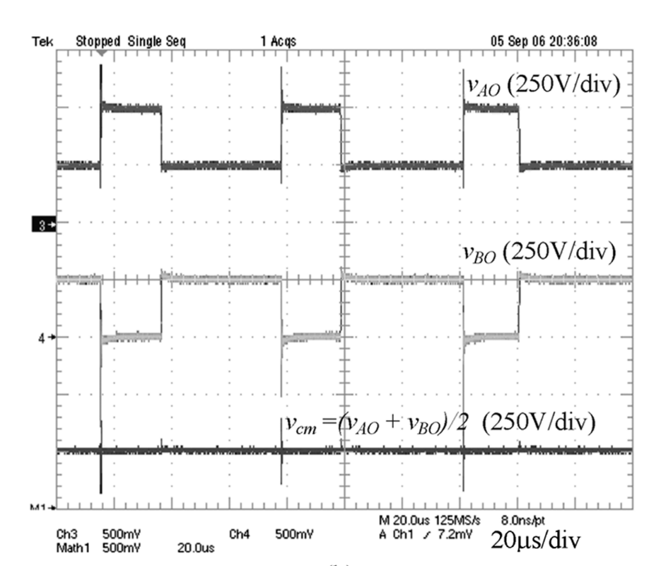
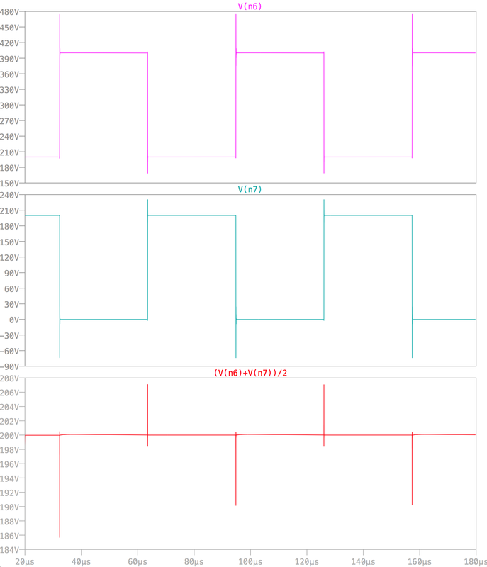
Common Mode Voltage and Respective Node Voltages
Research PaperIn this waveform set, the inverter was driven with a Vpv of 500V. The voltage at A switches between 250 and 500V. The voltage at B switches between 250 and 0V. Because of this switching pattern, the common mode voltage is constant at 250V except for some brief transients.
|
SimulationIn this waveform set, the inverter was driven with a Vpv of 400V. Node 6 and 7 is equivalent to node A and B. Similarly, the voltage at node 6 switches between 200 and 400V while node 7 switches between 200 and 0V. The common mode voltage is constant throughout this except for some brief transients.
|
|
|
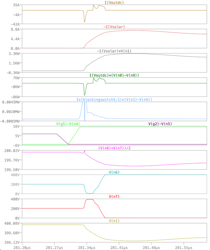
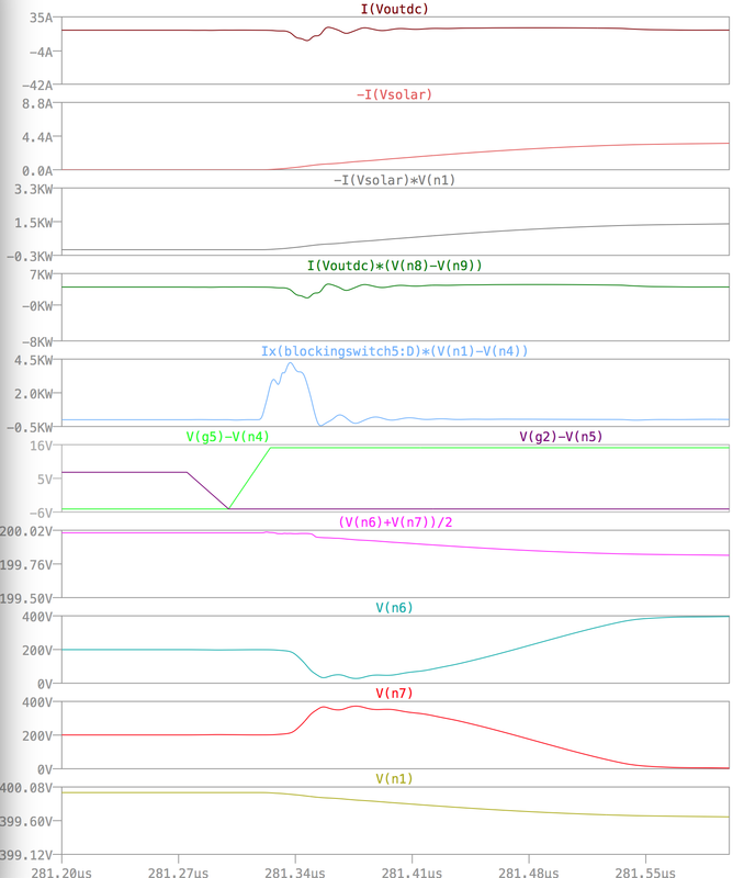
Switching Event for Two Transformerless Inverters
IGBTs and Si Diodes |
SiC FETs |
In the plots below, a single switching event is depicted. For this event, S2 and S3 turn off and S5 and S6 turn on. The dead time for the gate of S2 and the gate of S5 can be observed, along with the transient operation of the inverter with both sets of devices.
|
|